 Donald Sipes
580 California St., Suite 400
San Francisco, CA, 94104
Ultrafast Electronics and Optoelectronics
https://doi.org/10.1364/UEO.1997.UA6Public reporting burden for this collection of information is estimated to average l hour per response, including the time for reviewing instructions, searching existing data sources, qathenng and maintaining the data needed, and completing and reviewing the collection of information. Send comments regarding this burden estimate or any other aspect of this collection of information, including suggestions for reducinq this burden, to Washington Headquarters Services, Directorate for Information Operations and Reports, 1215 Jefferson '


![controlled Ti:Sapphire oscillator, which provides nearly transform limited 8-fs pulses. These pulses were amplified at a repetition rate of 1] kHz in a multipass amplifier pumped by the second harmonic of a Q-switched Nd: YLF laser [l]. The transform-limited output pulses have a duration of 20 fs, energy up to 300 uJ and a spectrum centered at 780 nm. The amplified pulses were coupled into a 160-zm-diameter. 60-cm-long fused-silica hollow fiber. The fiber was kept straight in a V-groove made in an aluminium bar which was placed in a pressurized chamber with fused-silica windows (1 mm thick) coated for broadband antireflection. The hollow fiber was filled with krypton at different pressures. By properly matching the input beam to the EH,,; mode of the fiber. an overall fiber transmission of 65% was measured. which is close to the value (~ 73 %) predicted by the theory. Figure 1. Spectral broadening in krypton at 2.1 bar and input peak power Pp= 2 GW. The spectrum of the imput pulses is shown as dashed curve.](https://figures.academia-assets.com/75105017/figure_002.jpg)


![Figure 7. Comparison of spectra of (a) soliton laser and (b) stretched pulse laser. The Noise Von der Linde [12] has pioneered a simple measurement of the amplitude fluctuations and timing jitter of a modelocked pulse train. The pulse train is detected and the RF spectrum of the detector current is recorded. The spectral components are](https://figures.academia-assets.com/75105017/figure_012.jpg)


![Figure 10. The stretched pulse sigma laser. version of the stretched pulse laser has been commercialized by Clark-MXR, Inc. Yet, in order to achieve the ultimate in environmental stability, the use of Polarization Maintaining (PM) fiber would be desirable. Unfortunately, the simple P-APM action based on the rotation of the polarization ellipse cannot be employed in such fibers. We have attempted to achieve P-APM action by interfering two Kerr-shifted polarization eigenmodes. These attempts failed on account of environmentally induced changes in the birefringence of the fiber. Eventually, a Sigma Laser similar to the one worked on by Duling et al. [14] proved successful. Our laser [15] differs from Duling’s in using different GVD’s in order to achieve stretched pulse operation (Fig. 10).](https://figures.academia-assets.com/75105017/figure_015.jpg)

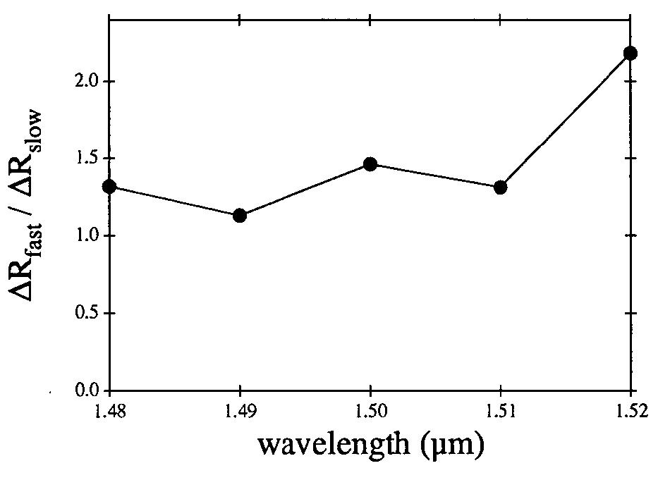
![radius of curvature high reflecting folding mirror provides astigmatic compensation and a 7.5 cm radius of curvature 0.2% output coupler focuses the cavity mode to a spot size of about 35 pm at the surface of the flat SBR. The structure of the SBR, (Figure 1) consists of a 99.5% reflecting Bragg mirror of alternating quarter-wave layers of GaAs and AlAs andtwo uncoupled Ing. 52 Gag,4g As/InP quantum wells located 15 nm from the top surface of a half-wave strain relief layer grown on the final layer of the Bragg mirror.[4-8] The excitonic absorption of the quantum wells is centered near 1500 nm. The output of a diode pumped Nd: YVQi CW laser (Spectra Physics) at](https://figures.academia-assets.com/75105017/figure_017.jpg)

![Figure 3. Plot of the pulsewidth (open markers, FWHM) and time-bandwidth product (solid markers) of the modelocked output with either one (circle), two (square) or three (triangle) pulses circulating in the cavity versus total cavity GVD. Bistable regions are indicated with dashed vertical lines. Simple CW cavity alignment produces self- starting modelocking of the laser believed to be initiated by the ultrafast saturation dynamics of the SBR.[6-8] With approximately 7 W of incident pump power, 200 fs pulses (FWHM assuming a sech2 pulseshape) are produced (see Figure 2). Due to the low cavity GVD and nonlinearities](https://figures.academia-assets.com/75105017/figure_019.jpg)


![polarization rotation, and the so-called “rejection port” of the laser is used to couple as much as 40 mW of average power in a single mode fiber [12]. Pulses with a bandwidth in excess of 70 nm are extracted from this laser. The spectrum is mapped onto the time axis by propagation through a single- -mode fiber with total dispersion oe v7 mM rr rr. a](https://figures.academia-assets.com/75105017/figure_051.jpg)


![technique that periodically alternates the fast and slow axes of the fiber to achieve repeated collisions between the contro! and signal pulses [11]. These collisions result in an accumulation of the net nonlinear collisional phase shift. The cross-splice is achieved by rotating one fiber’s birefringence axis 90° with respect to the other fiber before fusion splicing. Figure 1. Experimental setup for soliton collisions in a nonlinear optical loop mirror (NOLM). OPO is an optical parametric oscillator, 50/50 indicates a 3-dB PM fiber coupler, PBS indicates a polarizing beam splitter, 4/2 indicates a half-wave plate, and ® indicates a cross splice.](https://figures.academia-assets.com/75105017/figure_060.jpg)


![Figure 1. Block diagram of experimental arrangement “a The Raman effect on ultrashort optical pulses propagating in silica fibers and the resulting soliton self frequency shift effect have been quite well investigated [2,3]. An optical intensity dependent switch using the soliton self-frequency shift has also been reported [4]. Although the soliton self frequency shift effect is considered a detrimental effect in high bit rate communication systems since it is a potential source of jitter, its pulse-width and intensity dependent frequency conversion characteristics can be exploited to perform a new function, namely thresholding, for an ultrashort pulse CDMA receiver. A block diagram of the receiver is shown in fig. 1. Input pulses to the experiment are generated by a stretched pulse modelocked fiber ring laser [5] and are spectrally filtered to yield pulse durations of](https://figures.academia-assets.com/75105017/figure_063.jpg)


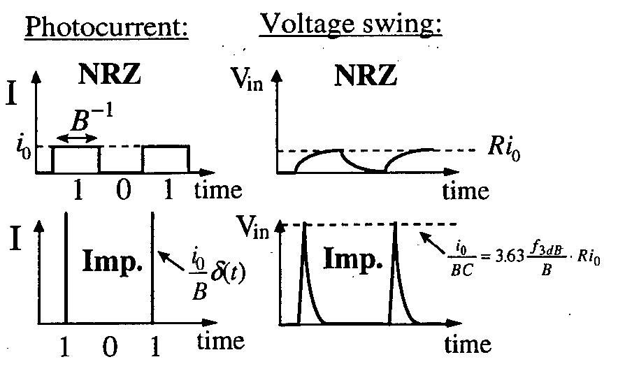
![Figure 1: Pictorial representation of NRZ and impulsively encoded optical data streams. T is the bit period. Non-return-to-zero (NRZ) coding, in which optical pulses occupy a full bit period, is the most widely used format in optical fiber communication. The popularity of NRZ stems, in part, from its minimum use of electronic bandwidth to modulate the output of a continuous-wave laser at a given bit rate. New transmitters using modelocked lasers are however being considered for which “impulsive coding” is amore natural format. Contrary to NRZ, the optical power of an impulsively encoded pulse train occupies only a small fraction of the bit periods (Fig. 1). In this paper, we show that impulsive coding results in better receiver sensitivities compared to NRZ. We report impulsive sensitivity improvements as large as 4.7 dB and 5.8 dB for two pin-FET front-ends [1]. These values are in good agreement with a model of the response and noise characteristics of the receivers. They also confirm a](https://figures.academia-assets.com/75105017/figure_066.jpg)


![Figure 10: Sensitivity of the STZ-01 receiver front-end (87 MHz bandwidth) for NRZ and impulsive coding as a function of the output low-pass filter bandwidth. The curves are predictions from our model and the squares and circles are actual measurements for NRZ and impulsive coding respectively. affecting the signal, leading to better sensitivities. When the output filter bandwidth falls below the bit rate, the output voltage for isolated “1” and “0” cannot quite reach the top and bottom rails, leading to inter-symbol interference. The reduction of the noise bandwidth is then increasingly offset by a reduction in signal, leading to a minimum in the sensitivity curve. The filter bandwidth at which this minimum occurs depends on the exact frequency dependence of the noise. It is 37 % of the bit rate when the corner noise frequency is zero, and 68 % of the bit rate when the quadratic noise term in eq.(4) is absent [1].](https://figures.academia-assets.com/75105017/figure_072.jpg)
![Figure 1: The dependence of optimized gain of fiber-optical amplifier on distance pumping radiation. The vector NSE describing parallel process in nonlinear media is also considered [2]. Soliton solutions in planar waveguides display interest- ing signal dynamics. Interaction of these soli- tons can be used as multiplexers and demulit- plexers in a number of potential soliton commu- nication applications. A large class of optimiza- tion problems in optimal control theory, and its applications to the signal processing and image processing is considered. Application of opti- mal control theory to eliminate timing jitter effect [9], [10], {11].The new results have inter- disciplinary character and include the soliton theory, theory of optimal control of distributed media and numerous applications to the math- ematical models of distributed systems, such as parallel and distributed computing.](https://figures.academia-assets.com/75105017/figure_073.jpg)


![The small signal response of VCSELs as a function of bias current was measured using a calibrated vector network analyzer. Air coplanar waveguide probes were used to drive the lasers and the output was collected into a cone-tipped 50 jum core diameter fiber. A New Focus photodector specified to have a -3dB response >30 GHz was connected through approximately 4 m of the multimode fiber. The modulation response of this system is plotted in Figure 3 for one laser at various bias currents. The -3dB frequency increases rapidly to 10 GHz at 1 mA and 15 GHz at 1.6 mA. The maximum observed -3dB bandwidth was 21.5 GHz at 4.8 mA as shown in the figure. The majority of the devices in this region of the wafer exhibited maximum bandwidths in excess of 19 GHz. For low biases, there is a droop of up to 2dB in the response at low frequencies (< 5 Ghz). The droop decreases at higher bias currents. Contributions to this droop may include the detector response, current crowding in the laser, or other bias dependent circuit effects. traditional damped resonator model modified Co Inciude a LOW Tequeley GIUUP See pees improve the fit. The resonant frequency, equivalent damping frequency (y/27), and -3dB bandwidth are plotted in Figure 4. At low bias currents, the bandwidth and resonant frequency increase in proportion to the square root of the current above threshold as expected from the conventional rate equation analysis. The rate of increase in this region yields a modulation current efficiency factor (MCEF) of 14.2 GHz/\mA which is slightly lower than the highest value we previously reported for oxide confined VCSELs with InGaAs quantum wells[1]. The resonant frequency increases steadily to 15 GHz at 2.7 mA and then becomes nearly constant. While multimode operation could limit the photon density in the fundamental mode and thus the resonant frequency of the fundamental, this is not expected to occur until 4 mA based on observation of the laser output spectra. Other possibilities include higher junction temperatures reducing the differential gain and current crowding reducing the overlap of the modulated carrier density and the mode.](https://figures.academia-assets.com/75105017/figure_081.jpg)


![[6] T. Itatani, T. Nakagawa, F. Kano, K. Ohta and Y. Sugiyama, Trans. IEICE vol. E78-C pp.73(1995).](https://figures.academia-assets.com/75105017/figure_098.jpg)

![Fig. 1. Schematic representation of the waveguide in cross section (upper part) and of the experimental setup for the electrooptic on-wafer pulse propagation measurements (lower part). Our TFMSLs (see Fig. 1) are fabricated on low- resistivity (5-8 Qcm) Si substrates. First, an 800- nm-thick Al ground-conductor metallization is de- posited onto the Si wafer by electron beam evapora- tion. Then, the insulator material, commercially avail- able Cyclotene 3022-46 from Dow Chemicals, is spin— deposited. Cyclotene is a resin based on Bisbenzocy- clobutene (BCB) momomers developed for applications in microelectronics such as passivation coatings and di- electrics for inter—chip connects in multi-chip modules [8]. It is cured for 60 minutes at 250°C in a N2 ambi- ent. After polymerization, the signal conductor with an integrated photoconductive (PC) switch is fabri- cated. First, a 500x500 ym? piece of 500-nm-thick lift-off LT-GaAs (LT: low-temperature-grown) is van— der-Waals bonded onto the polymer at the position in- tended for the PC switch (see below). After removal](https://figures.academia-assets.com/75105017/figure_100.jpg)
![Fig. 2. Electric signals probed at several positions z; (given in mm) on the 35-Q TFMSL (upper graph) and on the 70-0 TFMSL (lower graph). The signals are normalized to the maxi- mum of the first pulse. the electromagnetic signal with lattice vibrations whose propagation direction is oriented perpendicular to the wafer surface [13]. Reflection at the topside of the elec- trooptic crystal results in a standing-wave resonance.](https://figures.academia-assets.com/75105017/figure_101.jpg)
![Fig. 3. Frequency dependence of the effective permittivity of both TFMSLs. crease of €,,-¢7 with rising f when the cut-off frequency for the next highest mode is approached [2], [5]. The rise of €,er¢ for f — O results from the finite conductiv- ity of the metallization (skin effect) and is well known in the analysis of waveguides including low-—dispersive](https://figures.academia-assets.com/75105017/figure_102.jpg)


![Our switch configuration was not designed for EO measurements [3]. Nevertheless, we managed to get preliminary results by connecting the switch as a meander- type slot line. The signal was generated and measured entirely on the face of the switch structure. It propagated in](https://figures.academia-assets.com/75105017/figure_116.jpg)


![advanced laboratory technologies are required to achieve this data rate with the speed-critical circuits, as long as the other specifications are not essentially relaxed. Recent measurement results of mounted Si-bipolar chips are shown in Fig. 1 [5-7]. The circuits, again developed in cooperation between RUB and Siemens, are listed in the last column of Table 1. They were fabricated either with an improved laboratory version of the B6HF [8] (DEMUX), a former epitaxial-base technology (decision circuit), or a recent SiGe technology [9] (rest). All these ICs are used in an experimental 20 Gb/s TDM transmis- sion system [2]. Seong a For generating the eye diagrams in Fig. 1, the circuits were driven by a pseudo-random bit sequence generator with a word length of 2'°-1 bits [6]. The 60 Gb/s of the MUX, presented in [6], is the highest data rate ever gen- erated by an IC in any technology and the DEMUX [5], too, is far above the required data rate, despite of the slower (implanted base) technology applied. The excellent retiming capability of the DEMUX at the record input data rate of 46 Gb/s is demonstrated in Fig. 1b for an intentionally degraded input eye diagram. The output eye diagrams of the speed-critical circuits, transimpedance preamplifier and modulator driver, are given at 20 Gb/s. Here, the photo diode, which drives the amplifier, is modeled by an electrical network realized on the measu- ring substrate [10]. The high gain (58 dBQ) and low noise (estimated jy ~ 12 pA/ Hz ) of the transimpedance pre- amplifier (due to the high shunt feedback resistance of 900 2 in the first stage) as well as the comparatively high output voltage swing of the modulator driver (maximum values: 2.3 V for single-ended and 4.6 V for differential operation) are record values for 20 Gb/s Si ICs [7].](https://figures.academia-assets.com/75105017/table_003.jpg)


![Fig. 1. Schematic cross-sectional view of the fabricated DHBTs The DHBT epitaxial layer structure shown in Table 1 was grown by low-pressure metalorganic vapor phase epitaxy (MOVPE). The Zn doped p*-InxGaj.xAs compositionally graded base layer structure (In-As composition r, anging from 0.53 at the B/C interface to 0.47 at E/B one) was used to reduce the electron transit time and to lower t he extrinsic base contact resistivity. The potential drop across the graded base layer is 34 mV [9]. The InGaAs/InP comp tor layer structures are designed to improve t breakdown behavior without any significant cu ing effects, and to reduce the transit time [10]. thick n+-InGaAs layer was inserted to lower t contact resistivity. The 400-nm-thick InP subco osite collec- he collector rrent block- The 20-nm- he collector Hector layer was employed on behalf of the conventional InGaAs subcollector to lower the junction temperature because InP has over-one-order-higher thermal conductivity than InGaAs (0.68 versus 0.05 W/cm-K at 300 K) [11]. Thermal design is important for achieving high-density ICs.](https://figures.academia-assets.com/75105017/figure_155.jpg)
![The small-scale InP/InGaAs DHBTs were fabricated by self-aligned processing as reported previously [4,5]. A schematic cross-sectional view of the fabricated DHBTs is shown in Fig. 1. Using the lift-off Ti/Pt/Au emitter electrode metal as a mask, the E/B mesa-etching was carried out by a combination of Cly-based ECR-RIE and selective wet etch- ing (citric acid:H2O2:H20 and HCI:H3POq for the InGaAs and InP layers, respectively). The Pt/Ti/Pt/Au base electrode metal was then evaporated on the area including the emitter metal. The TLM measurements of the extrinsic base layers exhibited good sheet resistance of 616 Q2/square and specific contact resistivity of 2.4 x 10⁻⁷ Qcem2.](https://figures.academia-assets.com/75105017/figure_156.jpg)


![Ic at Vcg of 1.3 V for a DHBT with a 6-um? emitter. In spite of using the 420-nm-thick InP/InGaAs composite collector layers, the peak fy of 183 GHz is quite high, due to the 45- nm-thick In,Gaj-xAs graded base structure. Also, the de- pendences of fy and fmax on Vce at Ic of 3 mA and 6 mA for the same DHBT are shown in Fig. 7. fr's rapidly increases from alow Vcg of 0.6 V. The peak fmax is as high as 235 GHz at Ic of 6 mA since the extrinsic base resistivity of the In,Gay.xAs graded base layer is very low [9]. A further nar- rowing of the emitter width will enable our DHBTs to en- hance fmax values [12].](https://figures.academia-assets.com/75105017/figure_162.jpg)
![Figure 9 shows a block diagram of a regenerative receiver IC. The IC consists of a transimpedance-type preamplifier, cascode-type postamplifier, automatic offset controller (AOC), 90-degree delay, phase detector, lag-lead low-pass filter (LPF), hysterisis-comparator-type voltage-controlled os- cillator (VCO), master-slave D-type flip-flop (D-F/F). and output driver [13]. The VCO was designed to oscillate in the frequency range from 19 to 21 GHz. The reshaping is per- formed by a preamplifier, postamplifier, and AOC. The retiming is accomplished by a phase-locked loop (PLL) to extract clock signal. The D-F/F regenerates the NRZ data using the clock signal extracted from the PLL. Fig. 9. Block diagram of the regenerative receiver IC.](https://figures.academia-assets.com/75105017/figure_163.jpg)

![demultiplexed 10-Gbit/s data from the D-F/F [8]. Error-free operation is obtained for an input dynamic range of 13 dB. The power dissipation is 0.6 W at a supply voltage Veg of -5 VO](https://figures.academia-assets.com/75105017/figure_165.jpg)


![from 0 to Fs/2, oversampling (averaging) can improve the SNR by 3dB (0.5 bits) for every doubling of the clock rate. Using this technique, however, requires very high oversampling rates. For example, to achieve 10 bit resolution on a 50 MHz signal with a single bit ADC requires a 12.5 THz sample rate. A more practical solution to oversampling with a single bit ADC is to add a loop filter inside a feedback loop. This is the basic concept behind delta-sigma modulation [5].](https://figures.academia-assets.com/75105017/figure_180.jpg)


![Figure 1. Polarization-gate setup. Our scheme employs a polarization-gate beam geometry identical to that commonly used for optical switching using third-order optical-Kerr media [11]; however, a second-order type II BBO crystal replaces the third-order nonlinear-optical medium (Figure 1). The optical switch demonstrated here yields the same effect as the third-order Kerr gate — rotating the input beam polarization when a 45-degree-polarized gating pulse is present — and therefore shares its advantages of simple arrangement, collinear input and signal beams, and non-interferometric interaction. It is distinguished from the third-order optical-Kerr effect, however, by a strong angular dependence of the switching efficiency (we found an acceptance angle of](https://figures.academia-assets.com/75105017/figure_191.jpg)


![Figure 1. Scanning electron microscope picture of the epitaxial lift-off probe. The probe is 130 by 230 pum (at its widest points) by | um and consists of a Ti/Au interdigital MSM switch with fingersize and spacing of 1.5 um. The total switch area is about 30x30 um?. bulk substrate required a metallization process and several etching steps [2]. The teardrop shape of the LT GaAs layer (Fig.1) was formed by a phosphoric acid mesa wet-etch through the LT GaAs layer. A lift-off process was then used to deposit 500 A 3000 A of Ti/Au for the interdigital metal-semiconductor-metal (MSM) PC switch, electrode and tip. Lapping and backside etching, were used to release the probe from the GaAs bulk substrate. Ammonium hydroxide and hydrofluoric acid were used to etch the GaAs substrate and Alos;GajsAs etch-stop layer, respectively, while the front side was protected by black wax. Xylene was then used to dissolve the black wax separating the probes. A 5 x 5 mm’ die area produced 500 probes with a yield of 90%.](https://figures.academia-assets.com/75105017/figure_216.jpg)

![Figure 3. Temporal waveform resolved using the LT GaAs PC probe with integrated JFET source follower. The noise level measured at the baseline near t=0 ps is 15 nV/(Hz)!”. amplifier. This capacitance limits the modulation frequency of the beam directed at the transmission line gap to about | to 2 kHz. Typically, the sensitivity of photoconductive sampling below 1-kHz modulation frequency is several uV/(Hz)'. By introducing the amplifier with a smaller 3- pF capacitance, the charging time was reduced, increasing the allowed modulation frequency to tens of kHz. The important advantage of a high modulation frequency is that the 1/f noise due to gating laser fluctuations can be reduced [5]. However, above a specific frequency value (modulation frequency bandwidth) the measured signal falls below the actual signal under test.](https://figures.academia-assets.com/75105017/figure_218.jpg)


![While near-field scanning optical microscopy (NSOM) has attracted much attention for localized probing[6-8], sub- wavelength confinement of visible light was preceded by microwave demonstrations[9], and a wide range of contrast mechanisms in semiconducting, superconducting and biological materials and systems awaits exploration at the level of nanometer spatial resolution in the spectrum lying between DC and visible light[10]. Figure 1: 100 100 pm topographical scan of NLTL output section with the time-domain waveform of one 1.400 GHz cycle measured at the diode indicated by the arrow; the 10- 90 % falltime of the steepest edge is 30 ps, and the calibrated voltage scale is on the right. Incomplete contact metal liftoff can also be seen; this is otherwise difficult to detect under optical illumination. Reproduced with permission from Ref. [11}. Copyright 1997, American Institute of Physics.](https://figures.academia-assets.com/75105017/figure_221.jpg)
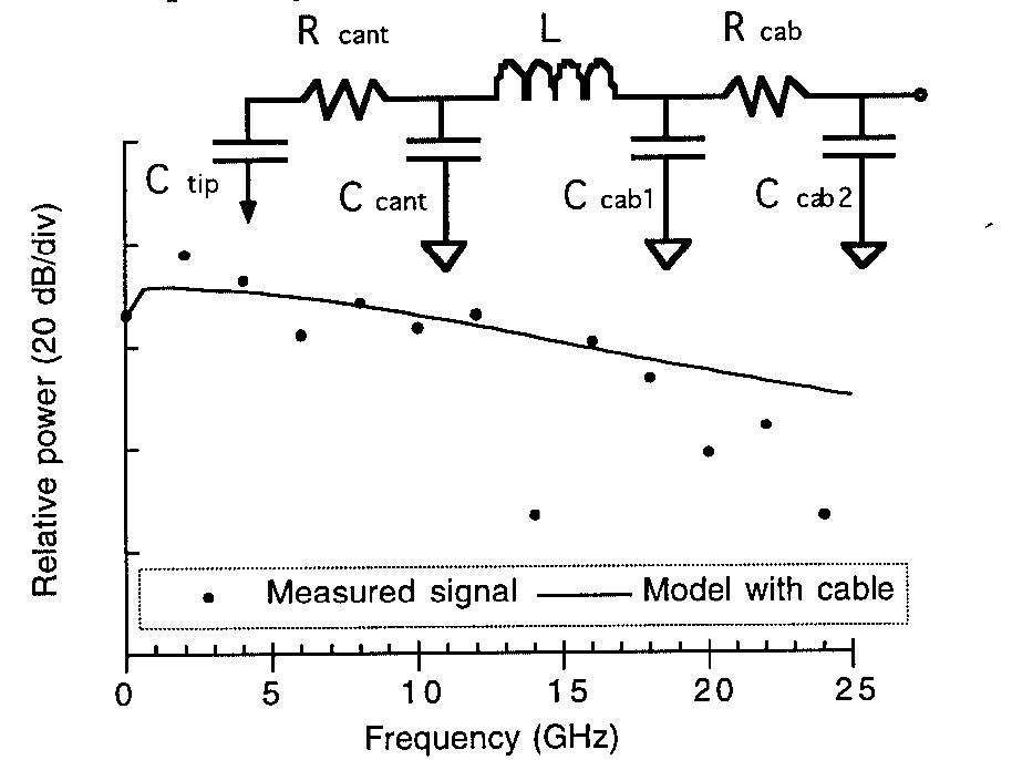
![Using a micromanipulator with a sharp-tipped tool, excess gold at the base of the cantilever can be removed. While this reduces the area for attaching the output wire, making attachment more difficult, it substantially reduces the capacitance between the metal and the conducting silicon body, in this case to ~ 30 fF, the capacitance due to the half-cylinder of metal on the cantilever alone. Using silver epoxy, 0.86 mm (outer diameter) semi-rigid coaxial cable[22] is anchored at the side of the probe body, minimizing its profile. An 18pm diameter gold bond wire is epoxied to the coax center conductor, then to the gold-coated base of the cantilever, then looped back on itself to the coax center conductor again, halving its inductance (Fig. 2). Approximately 50 mm of the coaxial cable extends from the mounting point to facilitate connection to a longer but lower-loss cable running to the signal measurement equipment. yo](https://figures.academia-assets.com/75105017/figure_222.jpg)

![Figure |. Schematic of system setup. One laser beam generates electrical pulse train. The other beam turns on optical switch on the probe. Figure | shows the system setup. The probe is supported by piezoelectric actuators in the x-, y-, and z-directions. The probe has a photo-conductive semiconductor switch (PCSS) on its thin-film cantilever[9]. One of the two electrodes of the PCSS is a sharp probe tip made of Pt, and](https://figures.academia-assets.com/75105017/figure_225.jpg)
![Figure 2. Top view of sample device. Two rectangles show the area ohserved hv SFOEM The cantilever is made of low temperature grown GaAs (LT-GaAs) and the material in the gap region between the two electrodes works as the PCSS [9]. An ultra-short optical pulse train from a mode locked Ti sapphire laser is used to turn the PCSS on and off. Since photo-excited carriers in LT-GaAs have an extremely short life (10-11), the response time of the PCSS is about I ps or shorter.](https://figures.academia-assets.com/75105017/figure_226.jpg)

![Figure 5. Simultaneously bserved images of interdigit coupler. Left is topographic image. Right is potential image. In the potential image, smal] waves with a short period have no meaning because they are due to 50 Hz noise from a power line. The upper electrode has a higher potentia and the lower one has a lower potential. In the GaAs substrate area between metal fingers, the measured potentia has no meaning. Because the substrate is an insulator, the charge sampled at the previous metallic point is maintained for a short time. In this measurement, the probe scans from left to right. Therefore, the substrate region of the potential image in Figure 5 seems as if it has the same potential as the left metal finger. The SFOEM is able to move the probe position anywhere in the observed area. We measured the time evolution of the potential at the hree points labeled A, B, and C in Figure 5. Figure 6 shows the results. The B curve seems to include the differential component of curve A. This is reasonable because the two electrodes have capacitive coupling. The C curve is almost similar to B. However, C is slightly](https://figures.academia-assets.com/75105017/figure_229.jpg)


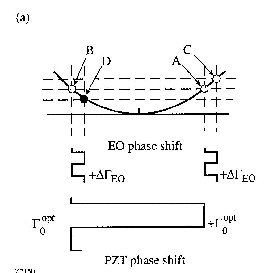


![Figure 5. Optimum optical bias point (operating point) To? and sensitivity factor f °" can be found, given quality p. This factor, also shown in Fig. 5, allows us to estimate the maximum attainable system sensitivity. Analysis of the optical system shows numerous sources that degrade interferometer quality (see Ref. [8]). In the remaining discussion, the values calculated for the system in Fig. 1 are p(a=0.94, b=0.085) = 1.044.](https://figures.academia-assets.com/75105017/figure_254.jpg)


![electro-optic sampling via the linear electro-optic effect (Pockels effect) offers a flat frequency response over an ultrawide bandwidth. Because field detection is purely an electro-optic process, the system bandwidth is mainly limited by either the pulse duration of the probe laser or the lowest TO phonon frequency of the sensor crystal. Further, since electro-optic sampling is purely an optical technique, it does not require electrode contact or wiring on the sensor crystal. Figure 2 shows the details of the sampling setup. Simple tensor analysis indicates that a <110> oriented zincblende crystal as a sensor gives the best sensitivity. The po parallel to the [i,-1 birefringence of the sensor crystal, via an applied electric fie optical probe beam passing through the crystal. The ellipticity modulation of the optical beam can then be po amplitude and phase of the applied electric field. The de arization of the THz beam and optical probe beam are 0] crystal direction. Modulating the d (THz), will modulate the polarization ellipticity of the arization analyzed to provide information on both the ection system will analyze a polarization change from the electro-optic crystal and correlate it with the amplitude](https://figures.academia-assets.com/75105017/figure_260.jpg)


![Figure 3: Coherence length versus THz frequency for ZnTe using optical excitation at 800 nm. The dotted line, calculated using Eq. (2), neglects the dispersion at optical frequencies. The solid line, calculated using Eq. (4), includes the effects of dispersion at optical frequencies. ZnTe crystal. Using a mode-locked Ti:sapphire laser producing 130 fs pulses at 800 nm, the THz electromagnetic transient produced by optical rectification in the ZnTe crystal was imaged into an identical ZnTe. The total separation between the emitter and detector was 50 cm. The measured field full width at half maximum (FWHM) pulsewidth of the temporal waveform of the THz electric field is approximately 270 fs. The corresponding amplitude spectrum, shown in Figure 4, exhibits a 3 dB bandwidth of ~ 2 THz. This is consistent with the data in Figure 3, where we find that the maximum frequency for obtaining a coherence length exceeding the thickness of the ZnTe crystals is ~2.25 THz. Thus, we would expect a rolloff in sensitivity for higher frequencies from the reduced interaction length. In addition to the limitations imposed by phase matching, the absorption caused by the dominant low-lying vibrational resonance in ZnTe at 5.4 THz [8] is expected to attenuate the high frequency components of the THz radiation.](https://figures.academia-assets.com/75105017/figure_280.jpg)

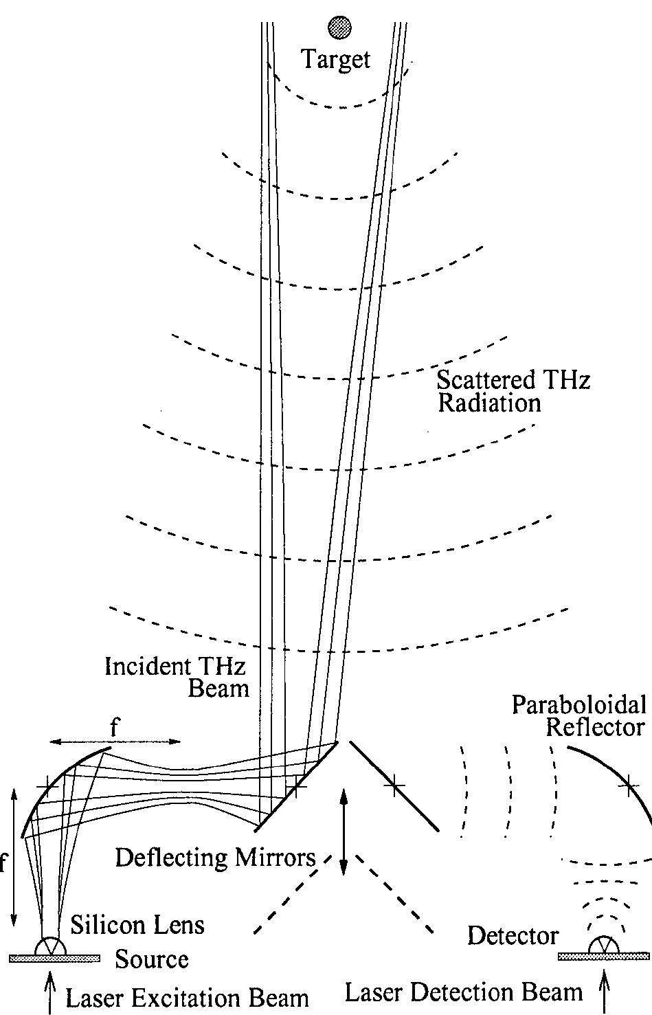

![Figure 3. (a) Measured time domain reflection (upper curve) compared to calculated reflection (ower curve) from a 1.96 mm dia. fused quartz cylinder at the beam waist (51 cm distance from the deflecting mirrors) of the silicon lens. The orientation of the cylinder axis is perpendicular to the incident electric field polarization. (b) Comparison of measurements (dots) and theory (solid line) on an expanded time scale for pulses B and C. (c) Corresponding measured (open circles) and calculated (solid line) normalized cross section. of the solid diclectric cylinder may be calculated exactly [9], and is shown as the solid line in Fig. 3c. Agreement is good from 0.2 to greater than 0.8 THz. In this figure the calculated cross section has a spectral resolution of 3.6](https://figures.academia-assets.com/75105017/figure_284.jpg)


![Figure2: a) THz waveforms before and after transmission through the near-field aperture. b) Normalized Fourier spectra of the data shown in a). factor is strongly frequency dependent. Both the larger focal diameter for the low-frequency components and their larger diffraction losses after passing the aperture lead to an effective spectral narrowing and a low-frequency cut-off at approximately 0.4 THz. Nevertheless there is significant signal amplitude for frequencies above 0.5 THz, corresponding to a wavelength of 12x dip. We also note that the cutoff is less sharp and at a much lower frequency than for a long waveguide with comparable diameter.[6] The spectral high-pass filtering of the signal also accounts for the changes of the THz waveform from a well-defined single-cycle pulse towards a more oscillating structure. In addition, both waveforms are slightly modulated due to residual water vapor absorption in the beam path.](https://figures.academia-assets.com/75105017/figure_293.jpg)


![Figure 4. THz radiation spectra obtained by Fourier transformation of the autocorrelation from a Polarizing Michelson interferometer. tricarbocyanine Iodide) in ethylene glycol. The Ti:sapphire laser cavity consists of a six-mirror cavity with an additional focus for a dye-jet, a 1% output coupler for monitoring femtosecond pulse formation, a single-plate birefringent filter as a tuning element, and a pair of high- dispersion SF6 Brewster prisms with 35-cm separation. A cw all-line Ar laser pumping source was operated at 12.5 Ww. ee EN Be Se Eee The autocorrelation trace and the spectrum were monitored with a rapid-scanning autocorrelator and an optical spectrum analyzer. 180-fsec pulses assuming a sech? shape were obtained with 3.9-nm spectral width at 768 nm, and these yielded a nearly transform-limited time and bandwidth product of 0.356. The average and peak output powers inside the cavity were 5.4W and 375 kW (80-MHz repetition rate). The peak power a the optical pulse irradiating SBR exceeded 8.3 MW/cm2, assuming a 1 mm beam diameter and considering the 80 degree incidence angle. The THz radiation was emitted in the transmitted direction and reflection direction. The transmitted THz radiation was picked off by a flat Al- mirror. The spectra of the THz radiation were obtained by Fourier transformation of the autocorrelation of the radiation from a Polarizing Michelson interferometer (Graseby Specac) as shown in Fig. 1. The interferometer was evacuated to avoid the possible absorption of water- vapor in the air. A liquid-helium-temperature cooled InSb bolometer (QMC model QFI/2) with subnanowatt sensitivity was provided for detection. For the lock-in detection, a mechanical chopper operated at 206 Hz was inserted in the cavity of the mode-locked laser. For this chopping frequency, a pulse-formation time of much less than 100 msec is short enough to reach the steady state. [11] Therefore the THz radiation from this laser can be considered to be modulated with a duty cycle of almost 50%. The average power of the radiation coupled to the interferometer was calibrated to be 2-3 nW in one beam.](https://figures.academia-assets.com/75105017/figure_305.jpg)


![After calculating E(t), the limited spectral band- width of the THz receiver antenna (~ 1.5 THz) is taken into account by convolution of the Fourier spectra of E(t) with the receiver spectral function [7]. Fig. 6. Comparison of the temperature dependence of the peak frequency (a) and the signal amplitudes (b) as obtained from the THz measurements (circles and triangles) and from calculations with the data of the optical experiments (full squares).](https://figures.academia-assets.com/75105017/figure_311.jpg)


![To demonstrate chemical recognition of gases and gas mixtures we have studied the polar gases H2O, NH3, HCI, and CH;CN in the pressure range between 0.3 and 13 kPa. Common for these species is that they have strong perma- nent dipole moments and hence they interact strongly with the terahertz field. Figure 2 shows a sample replica of a terahertz. waveform measured after propagating through NH; vapor at a pressure of 12.8 kPa. The impulse seen at zero delay excites some of the lowest lying transitions in the rotation-inversion spectrum of NH; [14]. Pronounced oscillations, due to the FID of the excited resonances, are seen at later time delays. Figure 2: Terahertz waveform resulting from the propagation through NH; vapor. The waveform is an average of 1000 real- time scans. The occurrences at 29 and 51 ps are due to reflections in the setup.](https://figures.academia-assets.com/75105017/figure_328.jpg)


![| Figure |: Simplified Four-wave mixing set-up. Two applications of four-wave mixing have emerged in recent years. The first is to use the amplitude versus detuning frequency information provided by the two new mixing products to characterize ultra-fast carrier dynamics and the second is to use the phase conjugate relationship of the new waves to perform all-optical signal processing. Both application areas will be discussed [1]. In the first part of this presentation, we will review the motivations for applying four- wave mixing elements in optical telecommunications systems. Specifically their application to carrier spectral inversion for fiber dispersion compensation and to spectral translation of optical carriers in WDM systems will be discussed. Recent achievements in each of these areas will be reviewed including the current signal-to- -noise performance of FWM mixers. Results from record conversion systems experiments will be presented. These include the results in figure 2 showing the wavelength conversion of 10 Gb/s data over spans as large as 18 nm [2]. The figure inset shows the eye diagram for the maximum shift of 18 nm.](https://figures.academia-assets.com/75105017/figure_334.jpg)

![LIOTTA IOUS UIE PU Pe Mt More recently, we have considered the application of four-wave mixing to measurement of interwell carrier equilibration in multi quantum-well active layers [3]. For this work we have used the polarization selection rules associated with tensile and compressively strained quantum wells to induce spatially selective mixing. Transport of this mixing to neighboring wells is then probed selectively using again the polarization selection rules.](https://figures.academia-assets.com/75105017/figure_336.jpg)


![Figure 1. Experimental setup for time-resolved electroabsorption. The conventional pump-probe transmission setup is modified with additional bias modulation on the sample. The sample is placed in a closed circuit cryostat at 10 K. D1 and D2 are InGaAs-photodetectors. unambiguously disentangled. For the incoherent transport a differential transmission technique with bias modulation is employed, which allows to derive the pure EA signal without contribution of bleaching induced by the pump pulse. On the coherent time scale we observe Bloch oscillations in the transmission signal as reported in a previous study [6] in this material system. As a results of dynamical screening due to incoherent transport we observe that the period of the decaying Bloch oscillations is chirped.](https://figures.academia-assets.com/75105017/figure_347.jpg)


![n=2 conduction subbands gives rise to an absorption line centered at 4.7 um, [6] corresponding to a photon energy of 264 meV. The infrared transmission spectrum, measured near Brewster's angle, is shown in Figure 2 [7]. This transition energy is in good agreement with envelope function approximation [EFA] calculations [8]. The normal incidence, interband transmission, shown in Figure 3, shows the characteristic steps of a quasi-two- dimensional system [9]. Doping the MQW sample n-type partially bleaches and broadens the absorption edge for the n=1 (valence) to n=1 (conduction) subband transition [10]. The n=2 absorption edge is much less affected due to the negligible population in the n=2 subband; the Fermi energy is estimated to be approximately 60 meV above the bottom of the n=1 subband.](https://figures.academia-assets.com/75105017/figure_354.jpg)


![Figure 6. Effect of Be-doping and 500°C post-growth anneal on nonlinear absorption recovery. Pulse energy density = 40 fI/um2. The low-excitation (40 fJ/um*) normalized differential transmission data of Figure 6 reveal that the combination of LTG and Be-incorporation can be used to engineer the absorption recovery time in the MQW material. The STG material exhibits a 1/e-recovery time of ~125 ps. Material grown at 200°C and Be-doped with a concentration of 5x10"” cm? exhibits a reduced 1/e-recovery time of 17 ps. Increasing the Be doping to 2x10"* cm® further decreases the recovery time to 600 fs. We note that this recovery- time estimate is not significantly reduced by PIA effects since the free-carrier lifetime in this material was independently determined to be sub-ps by far-infrared THz measurements using the technique described in [10]. Following a post-growth anneal (500°C for 30 min), the low- and high-doped recovery times increase to 24 and 2.5 ps, respectively. The apparent resolution difference of the](https://figures.academia-assets.com/75105017/figure_363.jpg)


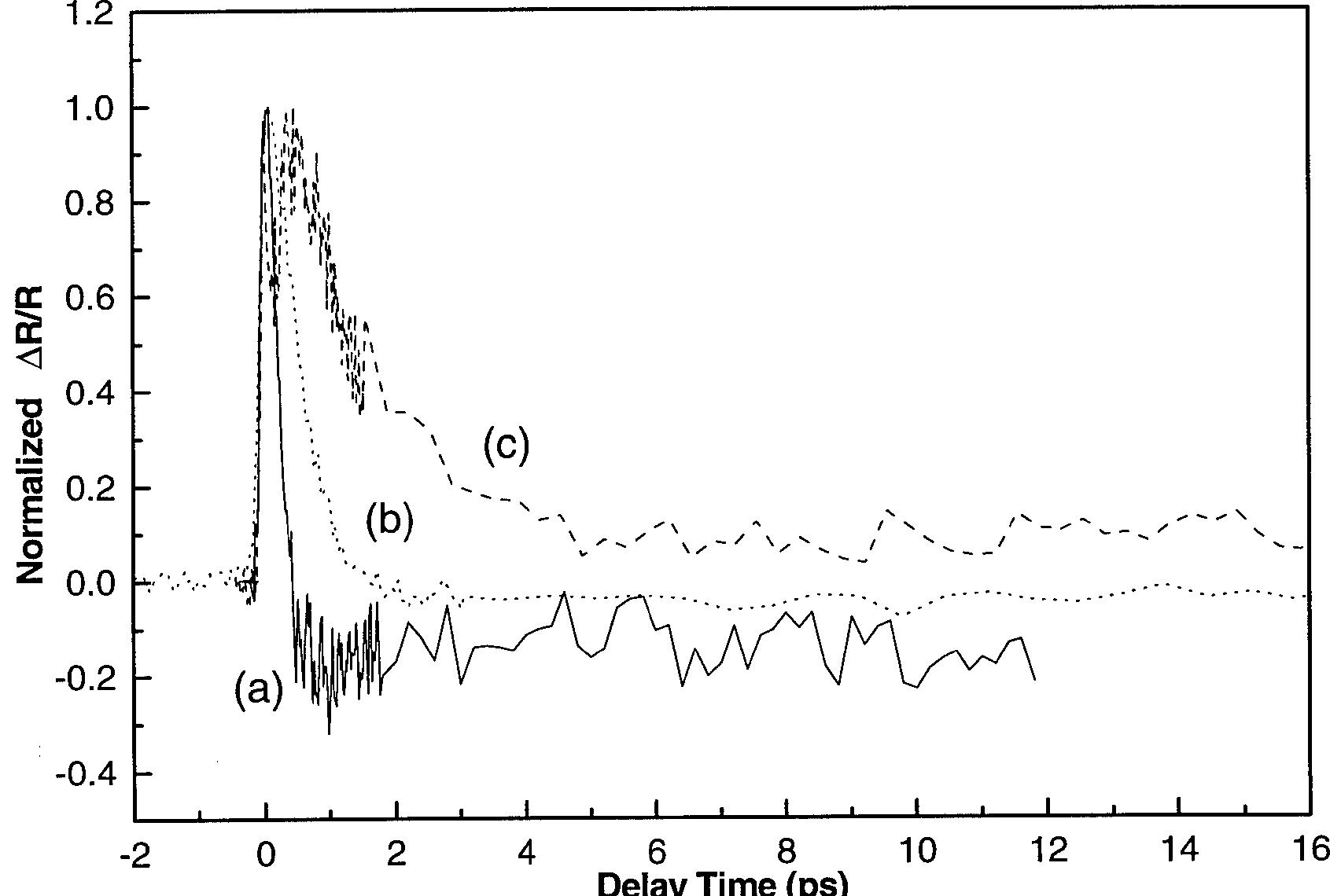
![Figure 3. The differential signal and the fit curves for the 210°C-grown GaAs sample with pump-pulse energies of 1 nJ, 12 nJ and 40 nJ. The inset shows more clearly the increased initial decay rate in the high-fluence measurement. The Auger rate in pure crystals is strongly limited by mo- mentum conservation requirements. [5] From our data we estimate the Auger coefficient to be on the order of 107?° cm® s~!, several orders of magnitude larger than the es- timated values for normal GaAs. We believe momentum conservation is relaxed in the 210°C-grown GaAs by the large concentration of defects that reduce the crystalinity. This relaxation creates a much wider range of momentum states into which the Auger-excited electrons may scat- ter, resulting in a drastically increased Auger rate.](https://figures.academia-assets.com/75105017/figure_367.jpg)


![Figure 6: Time resolved transient spectroscopy of 350°C grown GaAs. For the experimental conditions AT is proportional to the conductivity as is shown to be Drude-like within Ips of excitation. From the Drude model fit to the above data, the observed momentum relaxation time (ty) of the excited carriers is much smaller (~180fs+50fs) than the capture time. This is in excellent agreement with the value reported earlier in the literature [19].](https://figures.academia-assets.com/75105017/figure_373.jpg)
![TABLE I. Electron capture time (in ps) as obtained from our best fit for the 1pm thick LTG layer. The relative electron mobility also extracted from the model is shown in [] brackets.](https://figures.academia-assets.com/75105017/table_007.jpg)
