TOPICAL REVIEW: Black silicon method X: a review on high speed and selective plasma etching of silicon with profile control: an in-depth comparison between Bosch and cryostat DRIE processes as a roadmap to next generation equipmentJ Micromechanic Microengineer, 2009
An intensive study has been performed to understand and tune deep reactive ion etch (DRIE) processes for optimum results with respect to the silicon etch rate, etch profile and mask etch selectivity (in order of priority) using state-of-the-art dual power source DRIE equipment. The research compares pulsed-mode DRIE processes (e.g. Bosch technique) and mixed-mode DRIE processes (e.g. cryostat technique). In both techniques, an inhibitor is added to fluorine-based plasma to achieve directional etching, which is formed out of an oxide-forming (O2) or a fluorocarbon (FC) gas (C4F8 or CHF3). The inhibitor can be introduced together with the etch gas, which is named a mixed-mode DRIE process, or the inhibitor can be added in a time-multiplexed manner, which will be termed a pulsed-mode DRIE process. Next, the most convenient mode of operation found in this study is highlighted including some remarks to ensure proper etching (i.e. step synchronization in pulsed-mode operation and heat control of the wafer). First of all, for the fabrication of directional profiles, pulsed-mode DRIE is far easier to handle, is more robust with respect to the pattern layout and has the potential of achieving much higher mask etch selectivity, whereas in a mixed-mode the etch rate is higher and sidewall scalloping is prohibited. It is found that both pulsed-mode CHF3 and C4F8 are perfectly suited to perform high speed directional etching, although they have the drawback of leaving the FC residue at the sidewalls of etched structures. They show an identical result when the flow of CHF3 is roughly 30 times the flow of C4F8, and the amount of gas needed for a comparable result decreases rapidly while lowering the temperature from room down to cryogenic (and increasing the etch rate). Moreover, lowering the temperature lowers the mask erosion rate substantially (and so the mask selectivity improves). The pulsed-mode O2 is FC-free but shows only tolerable anisotropic results at -120 °C. The downside of needing liquid nitrogen to perform cryogenic etching can be improved by using a new approach in which both the pulsed and mixed modes are combined into the so-called puffed mode. Alternatively, the use of tetra-ethyl-ortho-silicate (TEOS) as a silicon oxide precursor is proposed to enable sufficient inhibiting strength and improved profile control up to room temperature. Pulsed-mode processing, the second important aspect, is commonly performed in a cycle using two separate steps: etch and deposition. Sometimes, a three-step cycle is adopted using a separate step to clean the bottom of etching features. This study highlights an issue, known by the authors but not discussed before in the literature: the need for proper synchronization between gas and bias pulses to explore the benefit of three steps. The transport of gas from the mass flow controller towards the wafer takes time, whereas the application of bias to the wafer is relatively instantaneous. This delay causes a problem with respect to synchronization when decreasing the step time towards a value close to the gas residence time. It is proposed to upgrade the software with a delay time module for the bias pulses to be in pace with the gas pulses. If properly designed, the delay module makes it possible to switch on the bias exactly during the arrival of the gas for the bottom removal step and so it will minimize the ionic impact because now etch and deposition steps can be performed virtually without bias. This will increase the mask etch selectivity and lower the heat impact significantly. Moreover, the extra bottom removal step can be performed at (also synchronized!) low pressure and therefore opens a window for improved aspect ratios. The temperature control of the wafer, a third aspect of this study, at a higher etch rate and longer etch time, needs critical attention, because it drastically limits the DRIE performance. It is stressed that the exothermic reaction (high silicon loading) and ionic impact (due to metallic masks and/or exposed silicon) are the main sources of heat that might raise the wafer temperature uncontrollably, and they show the weakness of the helium backside technique using mechanical clamping. Electrostatic clamping, an alternative technique, should minimize this problem because it is less susceptible to heat transfer when its thermal resistance and the gap of the helium backside cavity are minimized; however, it is not a subject of the current study. Because oxygen-growth-based etch processes (due to their ultra thin inhibiting layer) rely more heavily on a constant wafer temperature than fluorocarbon-based processes, oxygen etches are more affected by temperature fluctuations and drifts during the etching. The fourth outcome of this review is a phenomenological model, which explains and predicts many features with respect to loading, flow and pressure behaviour in DRIE equipment including a diffusion zone. The model is a reshape of the flow model constructed by Mogab, who studied the loading effect in plasma etching. Despite the downside of needing a cryostat, it is shown that—when selecting proper conditions—a cryogenic two-step pulsed mode can be used as a successful technique to achieve high speed and selective plasma etching with an etch rate around 25 µm min-1 (<1% silicon load) with nearly vertical walls and resist etch selectivity beyond 1000. With the model in hand, it can be predicted that the etch rate can be doubled (50 µm min-1 at an efficiency of 33% for the fluorine generation from the SF6 feed gas) by minimizing the time the free radicals need to pass the diffusion zone. It is anticipated that this residence time can be reduced sufficiently by a proper inductive coupled plasma (ICP) source design (e.g. plasma shower head and concentrator). In order to preserve the correct profile at such high etch rates, the pressure during the bottom removal step should be minimized and, therefore, the synchronized three-step pulsed mode is believed to be essential to reach such high etch rates with sufficient profile control. In order to improve the etch rate even further, the ICP power should be enhanced; the upgrading of the turbopump seems not yet to be relevant because the throttle valve in the current study had to be used to restrict the turbo efficiency. In order to have a versatile list of state-of-the-art references, it has been decided to arrange it in subjects. The categories concerning plasma physics and applications are, for example, books, reviews, general topics, fluorine-based plasmas, plasma mixtures with oxygen at room temperature, wafer heat transfer and high aspect ratio trench (HART) etching. For readers 'new' to this field, it is advisable to study at least one (but rather more than one) of the reviews concerning plasma as found in the first 30 references. In many cases, a paper can be classified into more than one category. In such cases, the paper is directed to the subject most suited for the discussion of the current review. For example, many papers on heat transfer also treat cryogenic conditions and all the references dealing with highly anisotropic behaviour have been directed to the category HARTs. Additional pointers could get around this problem but have the disadvantage of creating a kind of written spaghetti. I hope that the adapted organization structure will help to have a quick look at and understanding of current developments in high aspect ratio plasma etching. Enjoy reading... Henri Jansen 18 June 2008
 Professor Dr. Loutfy H . Madkour
![Fig. 2. Aluminum metal film stack and common issues in etching processes [21, 22]. For etching process requirement, a metal etch film stack and common issues are shown in Fig. 2](https://figures.academia-assets.com/38623301/figure_001.jpg)
![Fig. 1. The relationship of chamber materials, etching processes, precision wet cleaning and etch byproducts in a plasma etching chamber [21, 22, 35, 36].](https://figures.academia-assets.com/38623301/figure_002.jpg)


![In pattern A, chamber materials can be etched/sputtered by plasma uniformly. The etch rate can be very low or very high. The etch rate depends on the plasma chemistry, process recipe, and materials. For example, high purity Y2O3 has showed very high plasma resistance in both Metal and Silicon etch processes. A uniform corrosion/ erosion pattern is observed [21, 22, 25, 30]. For anodized aluminum, a very high corrosion/erosion rate is observed under BCl3-containing plasma during metal etch processes. In fact, an anodized aluminum film with a 75 um in thickness (hot deionized water sealed) can only hold up to 1,800 wafers in some etch process recipes in production. This became a severe problem on the lifetime of anodized aluminum in aluminum etch processes. For Silicon etch processes, the lifetime of anodized aluminum has no issue because there is no obvious attack of reactive gases to anodized aluminum in Silicon etch processes. The only concern is the formation of AIOF on anodized aluminum surface when SF¢ and NF; are used in the etching processes. The formed AIOF can either have chamber particle issue or cause etch process shift due to the surface impedance change on anodized aluminum surface. The wet cleaning to fully remove AIOF film on anodized aluminum surface is very critical to achieve a consistent and reliable etching performance on wafer fabrication. Fig. 5 shows an anodized aluminum metal etch chamber after 1,800 wafer fabrication in production. The anodized aluminum is fully removed under Cl2./BCl3 high density plasma [21, 22, 25, 30]. The major attack of anodized aluminum is due to the chemical reaction between BCl3 and AlsO3 under the high density plasma. The reaction rate of the attack to anodized aluminum highly depends on the gas concentration of BCl3 and the plasma density. Chamber erosion test indicates that Clz has little attack to anodized aluminum [21, 22, 25, 30]. The high density plasma reaction rate of BCl3; with anodized aluminum or high purity alumina at different flow is shown in Fig. 6. The high reaction rate occurs on chamber top window due to both high density plasma and gas flow. On the chamber wall, the reaction](https://figures.academia-assets.com/38623301/figure_005.jpg)
![Fig. 6. The maximum reaction rate of AlxO3 at different BCl3 gas flow under high density plasma [21, 22, 25, 30]. rate of BCl3 with Al:O3 is almost a liner relationship, but the reaction rate is much lower than that on the chamber top window. It also indicates that without BCl3 flow, the reaction rate of Clo plasma has almost no attack to anodized aluminum or to high purity alumina. In the plasma reaction rate study, the total flow is fixed as of 205 sccm. The Argon gas flow is fixed at 40 sccm. The test starts at 165 sccm Cl: flow and zero flow of BCls, then 155 sccm Clo flow and 10 sccm BCI; flow, until the final flow of Cl: is 85 sccm and BCl3 flow is 80 sccm. The test coupons are either on chamber top window or on the chamber wall. Nine different types of anodized aluminum and high purity alumina are used in the test [21, 22, 25, 30]. The reaction rate is in the unit of mils per RF hour.](https://figures.academia-assets.com/38623301/figure_006.jpg)


![Fig. 12. Wet cleaning compatibility test of four configurations of boron carbide coated rings. The wet cleaning compatibility of four configurations is also tested by soaking the large size B,C coated rings in saturated AlCl; solution at pH=0 for 90 minutes, then put the rings in an environmental chamber to monitor the time when boron carbide coating starts to peel off. The test sequence is shown in Fig. 12 [25].](https://figures.academia-assets.com/38623301/figure_011.jpg)
![Fig. 11. After plasma etching for 200 RF hours, Boron carbide coated anodized aluminum sealed with HL126 sealant provides the best corrosion in all configuration. and fast in comparison with ASTM standard salt spray test method [45, 46]. The test results show that boron carbide coating on anodized aluminum and sealed with HL126 provide the best corrosion resistance among the four configurations as shown in Fig. 11 [25].](https://figures.academia-assets.com/38623301/figure_012.jpg)
![n order to qualify boron carbide coating as a new chamber material, many aspects have to e considered. One of the concerns is the impact to ICF (ion current flux). Three onfigurations are considered and compared in the etching chamber. The ICF of anodized luminum. chamber is used as the baseline. Boron carbide coatings on bare aluminum or on inodized aluminum are studied through ICF measurements. The results showed that the hree configurations have the compatible ICF. The results of ICF measurements are shown n Fig. 13 [21, 22, 25, 30].](https://figures.academia-assets.com/38623301/figure_013.jpg)


![The new boron carbide coating has been introducing to worldwide wafer fabrication for over 10 years with over 1,000 chambers introduced to wafer fabrication in IC industry. The chamber lifetime has demonstrated to improve from the worse case as of 60 RF hours (1,800 wafers) under BCl3/Cl) etching plasma to over 4,000 RF hours or longer in semiconductor wafer fabrication in the world. It also demonstrates that the chamber materials play a critical role in semiconductor etching equipment, particularly, for the cost reduction. A short comparison of anodized aluminum and born carbide coating is highlighted in Table 4 [21, 22, 25, 30]. Anodized aluminum has been using as the major etching tools surface coatings since 1980. It still received a lot of applications in plasma etching tools because of its low cost, easy to manufacture, easy to make large or small sizes of the parts, wide applications, easy to refurbish, and achieving good quality control at different suppliers in the world. Therefore, the study of anodized aluminum has always been a major task for the major semiconductor etching tool manufacturers. For high purity Y2O3 thermal spray coating, it has been qualified and applied as one of the major chamber components in plasma etching tools in the past 10 years. It is still one of the major materials as coating or as a solid sintered material which is used in plasma etching tools. At Lam Research Corporation, great attentions have been paid in the improvements and the new development of anodized aluminum and Y2Os coatings.](https://figures.academia-assets.com/38623301/table_001.jpg)
![Fig. 20. The typical interface model of anodized aluminum with a hot DI water seal. The principal crystallographic defects are (1) vacancies: Vo'and Vm* for MOx;2; (2) interstitials: O; and Mix*. In fact, oxide films can be described as exponentially-doped semiconductor junctions. The fundamentals and process optimization of anodized aluminum have been studied thoroughly by Brace, Thompson, Wood, Mansfeld, and recent years by Shih through the comprehensive studies of anodization of different aluminum alloys, different anodization processes, and different manufacturing processes [51 - 60]. The interface model of anodized aluminum with hot DIW seal has been described by Mansfeld, Kendig, Shih and others [61- 72] as shown in Fig.20.](https://figures.academia-assets.com/38623301/figure_020.jpg)
![The overall impedance and HCI bubble test results are shown in Table 5. EIS data of three test coupons after immersion in 365 days in 3.5wt% NaCl solution are analyzed using the software written by Shih and Mansfeld called “ANODAL” [63-69].](https://figures.academia-assets.com/38623301/figure_021.jpg)
![In Table 6, @ is called frequency dispersion which is related to surface inhomogeneties with different dimensions [83]. Chi-sq is the fitting error between the experimental data and fitted data at each frequency. The detailed calculation is shown as below [84] and is the sum of the fitting error at each frequency multiplying 100 and dividing the total data points.](https://figures.academia-assets.com/38623301/table_002.jpg)

![Fig. 24. Acidic corrosion resistance of two test coupons of anodized aluminum. On the left, anodized aluminum does not show any acidic corrosion in two hours and on the right, anodized aluminum shows severe acidic corrosion after only 10 minutes immersion in the acid. For acidic corrosion resistance of anodized aluminum, HCl bubble test is an easy and very effective method to obtain the corrosion resistance. From Fig. 24 below, one can see the good and poor anodized aluminum under the solution of 5wt% HCl solution (28, 31-33, 44, 78]. On the left of Fig.24, there is no any hydrogen bubble generated under the attack of a strong acid within 2 hours immersion. It indicates a high quality of anodized aluminum. On the right of Fig. 24, anodized aluminum generates a lot of hydrogen bubbles in 5wt% HCl solution only after 10 minutes immersion in the acid. It indicates a poor anodized aluminum.](https://figures.academia-assets.com/38623301/figure_023.jpg)
![Fig. 23. TEM pictures of a standard type III hard anodization (left) and a mixed acid anodization (right) [80]](https://figures.academia-assets.com/38623301/figure_024.jpg)
![The HCl bubble test can be processed at any position of etching chamber before and after etching process. In Fig. 25, one process chamber is studied on its corrosion resistance in 5.0wt% HCl solution [76]. This method has received a wide application for the corrosion resistance study of anodized aluminum.](https://figures.academia-assets.com/38623301/figure_025.jpg)

![Assuming that C., Cpo and Cp are capacitances which represent the capacitances of Y2O3 coating layer, porous layer of anodized aluminum and barrier layer of anodized aluminum, respectively. The interface parameters can be obtained and the coating quality can be monitored. The interface model can be described as the following equation [28, 78].](https://figures.academia-assets.com/38623301/figure_027.jpg)
![In order to study Y2O3 coating on anodized aluminum, the following electrochemical cell configuration is used to study the overall impedance and interface model of the coated samples or parts as shown in Fig. 27 [28, 78].](https://figures.academia-assets.com/38623301/figure_028.jpg)


![With ex : interaction coefficient, [%X]: Concentration of the elements X in % It is obvious as per table 1 that specific elements will increase the nitrogen solubility (e.g. manganese), while others will reduce the solubility (e.g. silicon). This has not only an impact on the nitrogen pick up at remelting but also on the precipitation of inter-metallic phases in the solid state.](https://figures.academia-assets.com/38623301/figure_046.jpg)


![Fig. 12. TTT-diagram for the beginning of Cr2N-precipitation at different nitrogen contents. Curve is based on X5CrMnN18-12. [Rashev et al., 2003] ‘ig. 11. Precipitation of CryN in 18Mn18Cr at various nitrogen levels. [Uggowitzer, 1991]](https://figures.academia-assets.com/38623301/figure_054.jpg)

![Fig. 13. Breakdown potential of HNS and commercial stainless steels in various electrolytes. [ETE-11] A synergism of nitrogen and molybdenum is suggested by many authors [Mudali & Rai, 2004], [Pickering, 1988], [Pedrazzoli & Speidel, 1991]. Molybdenum shifts the metal dissolution to higher potentials which will consequently lead to an increased enrichment of nitrogen at the metal/oxide-interface. In this case, nitrogen can lower the current density below the critical value for pitting corrosion [Mudali & Rai, 2004].](https://figures.academia-assets.com/38623301/figure_056.jpg)
![Fig. 14. Influence of nitrogen on Current-density depending of a given alloy. [Pedrazzoli & Speidel, 1991]](https://figures.academia-assets.com/38623301/figure_057.jpg)

![Fig. 16. Critical Pitting Temperature (CPT) as a function of PRE. [Pedrazzoli & Speidel, 1991]](https://figures.academia-assets.com/38623301/figure_059.jpg)
![Fig. 18. MARC equation to rank various alloying element in regards to the alloy pitting resistance. | Speidel & Theng-Cui, 2003]](https://figures.academia-assets.com/38623301/figure_060.jpg)

![weight percent alloying elements C, N Fig. 19. Influence of various alloying elements on the pitting potential. [Pedrazzoli & Speidel, 1991]](https://figures.academia-assets.com/38623301/figure_062.jpg)
![The NHy+ - formation will increase the pH-value which support the repassivation. [Mudali & Rai, 2004] reports that NHg* - ions have been confirmed by XPS within the passivation layer.](https://figures.academia-assets.com/38623301/figure_063.jpg)

![Fig. 22. Precipitation of M23C6 and y-phase of a given alloy (17Cr-13Ni-4,5Mo) depending on annealing times and temperatures. [Gillessen et al., 1991] IGC is mainly driven by the depletion of Cr at the grain boundaries and/or the precipitations of carbides, usually M23Cs. Therefore, Carbon is supposed to be the main driver for IGC but also grain size, cold working and heat treatment have a significant influence on IGC.](https://figures.academia-assets.com/38623301/figure_065.jpg)
![It is commonly known that high alloyed steels are generally sensitive to SCC. The role of nitrogen against SCC has been discussed over the years but it appears that the positive effect of nitrogen is to be seen in a more oblique way. As previously discussed, nitrogen delays the carbide precipitation and avoids a local Cr depletion. Additionally, the crack growth velocity does not only depend on the actual Cr content, but also on the C content. The crack growth is much higher with increased C levels. It has been reported that nitrogen doesn’t have any influence on crack growth velocity at C > 0,5 % . The impact of carbon is therefore higher compared to that of nitrogen. [Pedrazzoli & Speidel, 1991]](https://figures.academia-assets.com/38623301/figure_066.jpg)
![Fig. 24. High precision bearing of Cronidur 30 [ETE-11]. Since its development in the early 1990s, Cronidur 30 (X30CrMo 15-1 plus 0,4 % nitrogen) has been approved as high performace alloy for aerospace applications such as spindles, shafts and bearings. It is used as material for helicopter bearings, flap traps, fuel pumps etc. It excellent corrosion resistance combined with a high hardenability of 60 HRC makes it unique. The alloy has become an important material to industries as cutleries and knifes, general engineering, medicals (since it is free of nickel) and powder metallurgy.](https://figures.academia-assets.com/38623301/figure_067.jpg)

![Fig. 27. Retaining ring. X8CrMnN 18-18 [ETE-11]. Fig. 26. Generator shaft with retaining rings, X8CrMnN 18-18 [ETE-11].](https://figures.academia-assets.com/38623301/figure_069.jpg)


![Table 1. Data showing the enhancement of the mechanical properties of Pb-free solders[9, 10].](https://figures.academia-assets.com/38623301/table_007.jpg)
![omposite solder by mechanically intermixing nano-Al2O3 particles into Sn0.7Cu Pb-f older, and this composite solder shows improved mechanical properties. The best ten: trength realized for the composite, which contains 1.5 wt.% alumina, far exceeds trength of the eutectic Sn-Pb solder. Many authors have studied the effect of adding sing valled carbon nanotubes [19] or multi-walled carbon nanotubes [20, 21] on the mechani roperties of nano-composite solders. The data on the enhancement of the mechani roperties of nano-composite solders collected from some of the literature are listed in Ta (13, 14, 16, 22, 23]. Here, it should be stressed that although the addition of nanopartic nto solder matrices can improve the creep behavior[24], the effects on the corros esistance and mechanical properties of the nano-composite solders cannot be ignored.](https://figures.academia-assets.com/38623301/figure_078.jpg)


![Fig. 3. Surface morphology changes of solder balls after the salt spray test for 96 hrs: (a) Sn Pb solder, and (b) SAC solder[39].](https://figures.academia-assets.com/38623301/figure_080.jpg)

![Unlike Sn-Pb joints, which have a dual phase structure and block the path of corrosion due to the existence of phase boundaries, the SAC305 joint is basically pure Sn with coarse islands of Ag3Sn and CugSns intermetallic precipitate (Fig. 5). A corrosion crack can propagate and lead to additional corrosion along the way, without interruption from the Sn phase structure. Although both materials show strong resistance to corrosion, the localized nature of the corroded area at critical locations causes significant degradation in Sn-Ag-Cu solder joints[40].](https://figures.academia-assets.com/38623301/figure_082.jpg)
![[41]. Thus, in the electronics industry, corrosion has become a significant factor in recent years because of the extremely complex systems that have been developed and the increasing demand on their reliability [42, 43]. For example, using Cu and Sn metals allows fine-pitch interconnections to be fabricated at relatively low cost. These features make Cu-Sn based SLID bonding very appealing for 3D stacked applications (Fig. 6) [44].](https://figures.academia-assets.com/38623301/table_009.jpg)
![Table 3. Aemf values for metals commonly used in microelectronics[4].](https://figures.academia-assets.com/38623301/figure_083.jpg)

![The joining of materials with solders generally results in a multi-layer structure in which IMC are formed between substrate and solders. Such a structure in a flip chip package is a galvanic couple. The galvanic corrosion behavior of the solder bump structures have a great effect upon reliability[45]. For instance, the galvanic current densities of the Sn solder with respect to the IMC CucSns and CusSn, and base Cu have been investigated (Fig. 7). It appears that Sn solder has a greater galvanic current density and thus is very subject to corrosion, and it is especially so in coupling with the formation of Cu3Sn layers than with Cu¢Sns layers. The galvanic current densities of the Sn37Pb solders of CugSn, Cu, and Cu¢Sns are about 38, 16, and 5 (pA/cm2), respectively.](https://figures.academia-assets.com/38623301/figure_084.jpg)

![Fig. 8. The potentiodynamic polarization curves of Sn37Pb solder, CugSns IMC, CusSn IMC, and pure Cu samples in a 3.5 wt.% NaCl solution [45].](https://figures.academia-assets.com/38623301/figure_086.jpg)

![thickness of the IMC layer was achieved with the addition of 1 wt% of nano-TiO, particles. The thickness of the CueSns IMC layer was reduced by 51%. The results indicate that the growth of the CugSns IMC layer at the solder/pad interfaces of Sn3.5Ag0.5Cu is depressed through the small addition of nano-TiO2 particles[58]. With the addition of 0.5- 1 wt% nano-TiO2 particles, fracture occurred in all of the solder joints as cracks propagated through the Sn3.5Ag0.5Cu composite solder balls, which ruptured mostly along the submicro Ag3Sn IMC and solder matrix, as shown in Fig. 13a, b. This phenomenon is similar to that occurring in Pb-free Sn0.7Cu composite solder BGA packages[59].](https://figures.academia-assets.com/38623301/figure_087.jpg)
![Fig. 11. SEM image of the (a) Sn3.5Ag0.5Cu solder and (b) Sn3.5Ag0.5Cu -1TiO, nano- composite solder[57].](https://figures.academia-assets.com/38623301/figure_088.jpg)

![Fig. 12. Morphology of intermetallic compounds formed at the interfaces of the as-reflowed solder joints: (a) Sn3.5Ag0.5Cu, (b) (a) magnifications ; (c) d Sn3.5Ag0.5Cu-0.75TiOz; (d) (c) magnifications [58].](https://figures.academia-assets.com/38623301/figure_090.jpg)
![To achieve high reliability, solder materials must have high resistance to corrosive conditions such as moisture, air pollutants from industry, and oceanic environments[54]. Although corrosion of solder alloys is not currently a major problem for electronic devices used in normal environments, it may be a problem when they are used in harsh environments, such as oceanic environments. However, there is a lack of information regarding the corrosion resistance of nano-composite solders in corrosive environments.](https://figures.academia-assets.com/38623301/figure_091.jpg)
![®corr : corrosion potential; Icorr: corrosion current density; Ob : breakdown potential; A® = Gcorr - Ob. resistibility or the stability of the passive film on the Sn3.5Ag0.5Cu composite alloy surface. The corrosion potential (@corr) of the Sn3.5Ag0.5Cu nano-composite solder is slightly more passive than that of the Sn3.5Ag0.5Cu solder. This implies that a finer grain size produces more grain boundaries, which act as corrosion barriers. On the other hand, the breakdown potential (®,) of the Sn3.5Ag0.5Cu nano-composite solders becomes much more passive with the addition of oxide nanoparticles. As Table 6 also indicates, the $n3.5Ag0.5Cu solders possess a higher pitting tendency (smaller A® value) than the Sn3.5Ag0.5Cu nano-composite solders. Rosalbino et al. reported that the pit formation at the surface of Sn-Ag-M alloys is due to the dissolution of the tin-rich phase [56]. In addition, the corrosion current densities were obtained by using the TAFEL extrapolation method. The corrosion current densities of the Sn3.5Ag0.5Cu solders and Sn3.5Ag0.5Cu nano-composite solders were very similar.](https://figures.academia-assets.com/38623301/table_012.jpg)
![Surface element concentration (wt. %) Table 7. Surface element concentration of different solders after potentiodynamic polarization tests[60].](https://figures.academia-assets.com/38623301/table_013.jpg)


![In addition, Li et al.[46] studied the corrosion properties of Sn-Ag, Sn—Ag-Cu, Sn-Cu, and SnPb solder in 3.5wt.% NaCl solution with different scanning rates, and their results showed that the corrosion product on the surface was tin oxide chloride hydroxide (Sn3O(OH)2Cl). In our case, the presence of such a surface layer, instead of a tin oxychloride layer, cannot be ruled out due to the detection limits of energy-dispersive spectroscopy. In order to understand the reaction during the corrosion products, XRD has been used to analyse the corrosion products on the surface after the polarization tests (Fig. 17). The results show that all the Sn3.5Ag0.5Cu and Sn3.5Ag0.5Cu solder materials have the same corrosion product, Sn30(OH)2Clz, which is a complex oxide chloride hydroxide of tin[67]. This further confirms that the corrosion product on the Sn3.5Ag0.5Cu composite solders is Sn30(OH)2Ch.](https://figures.academia-assets.com/38623301/figure_094.jpg)
![Fig. 17. XRD spectra of different solder materials after polarization tests[60].](https://figures.academia-assets.com/38623301/figure_095.jpg)

![Fig. 1 shows the anodic dissolution behaviour of alloys in 0.5 M H2SQu, while Table 2 summarizes relevant data. This figure reveals a well-defined passive region of 0 Vsue to 1.2 Vsue in all curves. All curves, except for the one at x = 0.25 (C-0.25), show a secondary passive region at 0.15 Vsu. This passivation is attributed mainly to the further oxidation or hydroxidation of the passive oxide film, thus altering the valence of Cr [18,19]. Fig. 1 also indicates that the secondary passive regions of C-0.50 and C-1.00 are more prominent than those of C-0 and C-0.25. This observation is due to the selective dissolution in the duplex FCC-BCC structure for C-0.50 and in the BCC-ordered BCC structure for C-1.00, as compared with C-0 and C-0.25 which are single FCC phase. In the active-passive transition region, different compositions at different secondary passivation potentials reveal different dissolution rates owing to a selective dissolution. This observation resembles that observed in duplex phase stainless steel [20,21].](https://figures.academia-assets.com/38623301/table_015.jpg)


![@ Anodic Tafel slope Ba in mV/ decade, the measured Tafel regions are with 40~50 mV of overvoltage. ’ Cathodic Tafel slope B. in mV/ decade, the measured Tafel regions are with 150~170 mV of overvoltage. ae See ae Se ee GSE ee ee ee ORs FRR Sena Ree Fig. 3 shows polarization diagrams of Al,CoCrFeNi alloys at various temperatures. A rising temperature decreased the Tafel slopes of anode (Table 3), increased Icon, and increased Ecorr and E; (the transpassive potential) slightly. The corrosion rate is directly related to loom, according to Arrhenius equation, Ico = A exp(-E,/RT) [13,26], where the pre-exponential factor A is generally independent of temperature and is a constant of alloys, where R denotes the gas constant, T denotes temperature, and E, denotes activation energy for corrosion. In the case of small experimental temperature range, E, is assumed to be independent of T. Consequently, E, can be obtained from In(Icorr) vs. 1/T plot. Fig. 4 shows such plots for the alloys and SS 304, indicating that E, increases with x. This finding suggests that the corrosion rate is more sensitive to temperature for a larger Al content than for a smaller Al content. The In(Icorr) vs. 1/T curves intersect with each other in a range of 23°C - 27°C. Beyond this temperature range, [corr increases with x. The situation is reversed at temperatures lower than 23°C, which is inconsistent with a situation in which E,s for all alloys increase with x from 20°C to 65°C. Hence, Ez, i.e., an intrinsic property of metal, and A, i.e., a surface property of metal, are determinative factors of Ico. While E, depends only on x, A depends on both x and temperature (Table 4). Therefore, although E, increases with x, A also increases with x. Combining the effects of E;and A explains the different corrosion behaviours of the alloys with an increasing x at temperatures exceeding 27°C and lower than 23°C. Thus, the performance of passive films, when Al is added, at higher temperatures becomes inferior to that without addition of Al. In determining Icon, A is more important than E, at temperatures exceeding 27°C, while E, is more important than A at temperatures lower than 23°C.](https://figures.academia-assets.com/38623301/table_017.jpg)


![Table 6. EDS analyses (at %) for alloys C-0, C-0.25, C-0.50, and C-1.00. Microstructures for not H25Q4-immersed alloys C-0, C-0.25, C-0.50, and C-1.00 are with single FCC, single FCC, duplex FCC-BCC, and BCC-ordered BCC phases, respectively [6]. Table 6 lists the EDS composition for each phase in different alloys.](https://figures.academia-assets.com/38623301/table_019.jpg)


![microstructure. The composition of BCC phase after alloy immersion is close to the overall alloy composition before immersion, indicating that the BCC phase is a corrosion-resistant phase. Moreover, the change in overall composition after immersion is attributed to the selective dissolution of Al and Ni in the ordered BCC phase of this alloy (Table 6). This selective corrosion in Al and Ni-rich phase in C-0.50 and C-1.00, which results in the corrosion attack on Al and Ni, is due to the large bonding in Al and Ni [37]. Alloys containing this bonding readily react with (OH)- and (SOu,)? to form Al and Ni complexes and dissolve in a sulfuric solution. Accordingly, after immersion, the remaining compound in the less corrosive-resistant Al and Ni-rich phase is an oxide, rich in Cr, in the residual passive film.](https://figures.academia-assets.com/38623301/figure_108.jpg)

![Fig. 14. (a) Iai, (b) Ipass, (c) Wioss, (d) Qt, (e) Re, and (i) Icorr values vs. Al content x plots. Ipass locate at the passive region of polarization curve. The same tendency for Ici, Ipass, ane Wiooss here indicates that the spontaneous passivation occurs for Al,CoCrFeNi, i.e., the oper circuit potential (OCP) is readily in the passive region of polarization curve. The above phenomenon can be attributed to the spontaneous passivation of pure Al in H2SOx [24]. EIS equivalent circuits reveal that the passive layers of AlxCoCrFeNi consist of an oxide layer and an adsorption layer mentioned in Section 3.3. Here, only parameters associated with the oxide layer, i.e., Q¢ and Rg, are discussed. The oxide layer thickness is evaluated by using the Helmholtz model mentioned above and denoted by d, as d = e&S/Q: where & denotes the permittivity of free space (8.85 x 10-74 F/cm), ¢ denotes the dielectric constant of the medium, and S denotes the surface area of the electrode. Assuming that ¢ and S for oxide layers of alloys are the same allows us to compare relative values of d for all samples by 1/Q;. Figs. 14(d)-(e), whose data were listed in Table 5, show the Q; and R; vs. x plot respectively. Both Qr and Ry decreases with x. This represents that d increases with A content x, and a thicker oxide layer implies a smaller value of impedance. Therefore, one car explain this phenomenon by considering both the thickness and the density of oxide layer Related study reported Al oxide easily forms a porous structure [25]. Hence, it is easily understood that in addition to causing a thicker oxide layer, Al promotes the dispersive anc porous oxide layer. In summary, Al has a negative effect to the passive parameters including Lori, Ipass, Wioss, and R¢, for AlxCoCrFeNi in H2SOu.](https://figures.academia-assets.com/38623301/figure_110.jpg)


![Properties of Graphite Sinters for Bipolar Plates in Fuel Cells Bipolar plates/interconnectors in fuel cells typically have channels on their surface to allow for the distribution of media to the electrodes [29]. The shape of channels and direction of flow of media might be different for the plate adjacent to anode compared to the plate near cathode. Media which flow in to both electrodes can be supplied by means of parallel channels, where media flow in one direction or channels where media are supplied to fuel cells with opposite directions. Another possible solution is that the media flow in with the direction transverse to the cell. The choice and optimization of the shape of the channels in bipolar plates affect the operation of the cell, particularly the degree of removal of products and distribution of gases to the surface of electrodes. The figure below presents bipolar plates with channels (Fig. 3). The essential effect on operation of the cell is from the depth of the channels, width of the channels, distance between spirals etc.](https://figures.academia-assets.com/38623301/figure_145.jpg)


![Table 8 contains the values of height and longitudinal parameters for 316L sintered steel and graphite-steel composites. The substantial impact on surface geometry in sinters is from the presence of graphite. In the case of rough surface, an insignificant contribution of contact surface is observed. It is essential for fuel cells that the surface of the material for these parts is smooth, which is obtained through polishing or covering the surface with a coating [59]. Graphite, as a material with high porosity is subjected to polishing in order to obtain the smooth surface.](https://figures.academia-assets.com/38623301/figure_161.jpg)


![Fig. 2. Wagner’s model of the transition from the internal to external oxidation of alloy A-B under the condition where only B can oxidize: a) B is less than the critical amount of B required for the transition and b) B is higher than the critical content of B required for the transition from the internal to external oxidation [44,45, 110-112].](https://figures.academia-assets.com/38623301/figure_166.jpg)

![For Fe-Cr alloy, X’ is calculated based on available data listed in the Table 1 (extrapolated from the literature [114,115] with do assumed to be 5 micron, and plotted it as a function of grain size in Fig 4. Figure 4 clearly shows that Cr required for such transition decreases substantially when grain size is below 100 nm.](https://figures.academia-assets.com/38623301/table_035.jpg)

![Table 2. Parabolic oxidation rate constants (k) values in g’cm“s*[12]](https://figures.academia-assets.com/38623301/table_036.jpg)
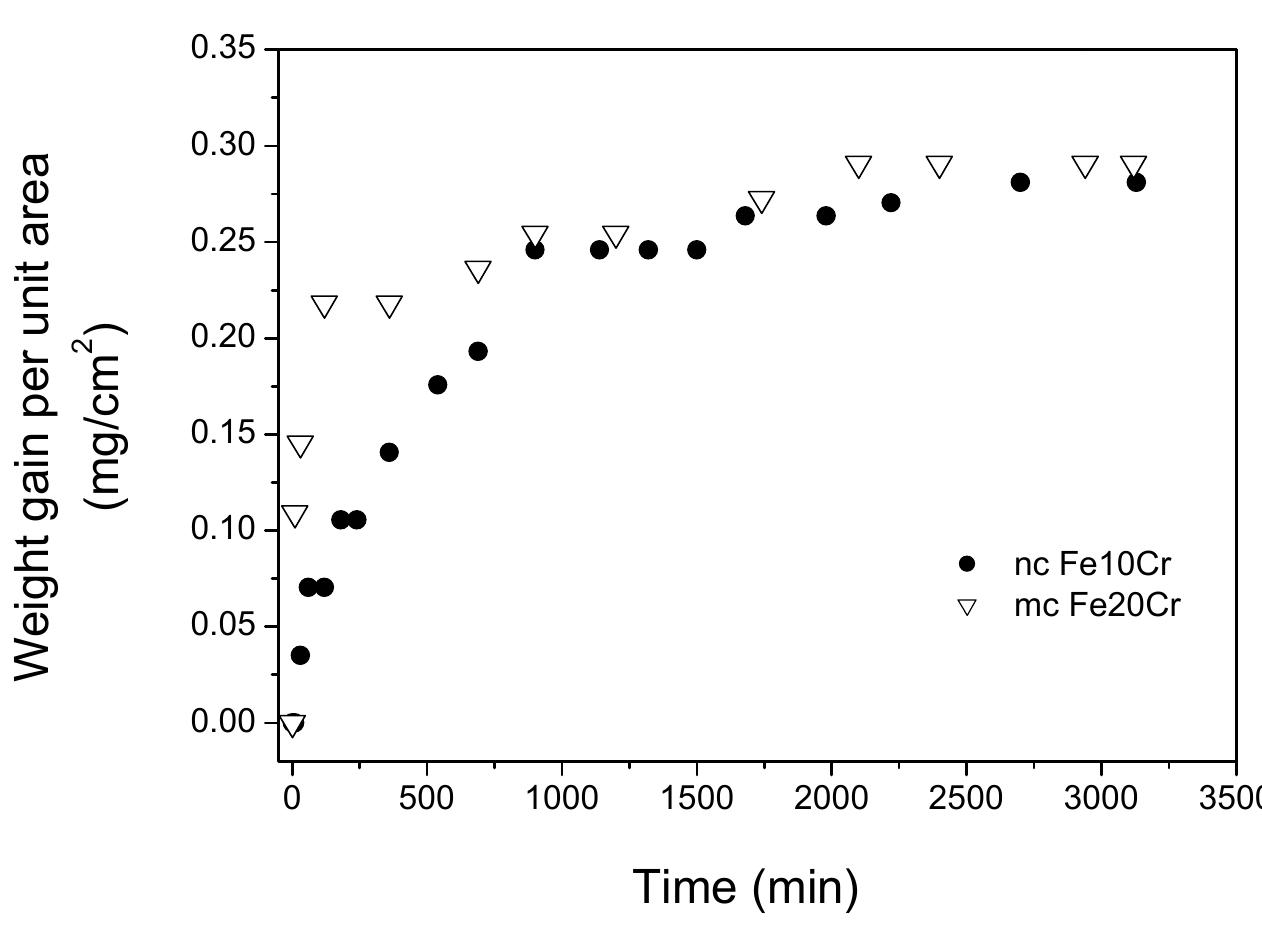
![Fig. 5a. Oxidation kinetics of nanocrystalline (nc) and microcrystalline (mc) Fe-10Cr alloys at 300°C as represented by weight-gain vs time plots for 3120 minutes [12,37,39]. Inset shows the zoom of the region representing initial periods of oxidation (up to 240 minutes of oxidation).](https://figures.academia-assets.com/38623301/figure_169.jpg)

![Fig. 5c. Oxidation kinetics of nanocrystalline (nc) and microcrystalline (mc) Fe-10Cr alloys oxidised at 300°C: weight-gain2 with time, suggesting parabolic kinetics for mc alloy but departure from parabolic kinetics for nc alloy [12,37,39].](https://figures.academia-assets.com/38623301/figure_171.jpg)
![Fig. 6a. Oxidation kinetics (weight-gain vs time plot) of nanocrystalline (nc) and microcrystalline (mc) Fe-10Cr alloys, during oxidation at 350°C for 3120 min in air [12,39]. Inset shows the zoom of the region showing initial periods of oxidation (up to 240 minutes of oxidation).](https://figures.academia-assets.com/38623301/figure_172.jpg)
![Fig. 6b. Oxidation kinetics of nanocrystalline (nc) and microcrystalline (mc) Fe-10Cr alloys oxidised at 350°C: weight-gain2 with time (up to 240 minutes) suggesting parabolic kinetic for both mc and nc alloys [12,39] Oxidation Resistance of Nanocrystalline Alloys](https://figures.academia-assets.com/38623301/figure_173.jpg)

![Fig. 7. Oxidation kinetics (weight-gain vs time plot) of nanocrystalline (nc) and microcrystalline (mc) Fe-10Cr alloys, during oxidation at 400°C for 3120 min in air [12,39]. Inset shows a zoom of the region of initial periods of oxidation (up to 240 minutes of oxidation).](https://figures.academia-assets.com/38623301/figure_175.jpg)
![Fig. 8. SIMS depth profiles for Cr the in the oxide scale developed during oxidation of nanocrystalline (nc) and microcrystalline (mc) Fe-10Cr alloys at 300°C for in air for 3120 minutes, using a Cameca ims (5f) dynamic SIMS instrument. SIMS parameters were: Cs* io primary beam (10 nA), depth profiling of craters of 250 um x 250 um area [12,39]. Oxidation Resistance of Nanocrystalline Alloys](https://figures.academia-assets.com/38623301/figure_176.jpg)
![Fig. 9. SIMS depth profiles for Cr the in the oxide scale developed during oxidation of nanocrystalline (nc) and microcrystalline (mc) Fe-10Cr alloys at 350°C for in air for 3120 min, using a Cameca ims (5f) dynamic SIMS instrument. SIMS parameters were: Cs* ion primary beam (10 nA), depth profiling of craters of 250 ym x 250 um area [12,39].](https://figures.academia-assets.com/38623301/figure_177.jpg)
![Fig. 10. SIMS depth profiles for Cr the in the oxide scale developed during oxidation of nanocrystalline (nc) and microcrystalline (mc) Fe-10Cr alloys at 400°C for in air for 3120 min, using a Cameca ims (5f) dynamic SIMS instrument. SIMS parameters were: Cs* ion primary beam (10 nA), depth profiling of craters of 250 um x 250 um area [12,39]. SIMS analysis as carried out in our previous work [12,39] provides a qualitative analysis of Cr enrichment of the surface. Based on such qualitative analysis of Cr content, a Cr2O03 oxide layer was proposed to develop in nanocrystalline alloy, whereas, it was proposed that a mixed Fe-Cr oxide layer forms in case of microcrystalline alloy. A Future study quantifying the Cr, Fe and O contents of oxide layer and their oxidation states using techniques such as X-ray photoelectron spectroscopy (XPS) must provide a better understanding of the effect of nanocrystalline structure on the chemical composition of oxide laver.](https://figures.academia-assets.com/38623301/figure_178.jpg)


![Fig. 15. Bode amplitude and phase spectra of circuit impedance and corrosion systems of Fe and $235]R steel in 0.5M NaCl solution determined experimentally (point line) and as a result of calculations (solid lines).](https://figures.academia-assets.com/38623301/figure_303.jpg)


![Fig. 1. Renewable resource based materials provide corrosion resistance against various corrodents. cost effectiveness, low toxicity, inherent biodegradability and environment friendliness They yield versatile materials through chemical transformations with plethora of applications, particularly in corrosion resistance against various corrodents [Fig. 1]. (Derksen et al., 1995, 1996; Gandini & Belgacem, 2002; Metzgr, 2001; Weiss, 1997; Ahmad, 2007).](https://figures.academia-assets.com/38623301/figure_313.jpg)


![Fig. 4. Structure of tannic acid. magnesium alloy obtained from solution containing TA and ammonium metavanadate. The corrosion resistance performance of these chromate free coatings was compared with the traditional chromate conversion coating. PD revealed that the said coating showed more positive potential and obvious lower corrosion current density relative to traditional chromate conversion coating; salt spray tests also showed the improved anticorrosive behavior of the former (Chen et al., 2008). In another report, mildly rusted steel surface were pretreated with TA based rust converters followed by the application of a Zn rich coating. The rust converters react with iron and rust to form a sparingly soluble iron tannate film on metal surface, which renders low pH adjacent to corroding interface by the diffusion of the unreacted acidic constituents of the rust converter in alkaline concrete solution. The low pH facilitates the formation of passive hydrozincite layer within 50h of exposure to chloride contaminated concrete pore solution relative to 150h for normal zinc coating without rust converter. The mechanism of film formation was investigated by EIS, Potential-time studies, Raman Spectroscopy, SEM, energy dispersive X-ray analysis [EDXA] and X-ray diffraction studies [XRD] (Singh &Yadav, 2008). Methacrylic derivatives of TA [m-digallic acid], toluylene 2,4-diisocyanate [TDI] and 2-hydroxyethyl methacrylate [HEMA] formed UV curable urethane coatings (in molar ratio 1:3:3). The formation occurred by the coupling reaction between TA and TDI followed by HEMA addition (Grassino et al., 1999).](https://figures.academia-assets.com/38623301/figure_316.jpg)


![/O is the single, largest, well-established, non-polluting, non-toxic, biodegradable family ised in coatings and paints, since primeval times particularly in corrosion resistance. Depending on their Iodine value [IV], VO are classified as non-drying, semi-drying and lrying, as indicated by their drying index [DI] (DI=linoleic%+(2linolenic%); “drying” VO : V>130 and DI> 70); “semi-drying” VO: 115<IV<130 and DI 65-75; “non-drying” VO : V<115; DI< 65). Usually, drying VO are used in coatings and paints. Drying VO are film ormers, ie., they have the tendency to form films over the substrate on drying by hemselves, without the use of any drier. In drying VO, drying occurs as a natural yhenomenon through auto-oxidation initiating from the active methylene groups on VO »ackbone. However, since these films are not tough enough to meet the desirable yerformance characteristics, VO are chemically transformed into several derivatives as volyesters, alkyds, polyesteramides, polyetheramides, polyurethanes (Fig. 8) and others, to neet the stringent environmental conditions. These have been further modified through hemical pathways including acrylation, vinylation, metallation, and others, for mprovement in their drying, gloss, scratch hardness [SH], impact resistance [IRt] , flexibility FL], and corrosion resistance of coatings produced therefrom. The presence of hydroxyls, sters, oxiranes, amides, carbonyls, metals, acrylics, carboxyls, urethanes, imparts good \dhesion to the substrate due to good electrostatic interactions with the metal substrate.](https://figures.academia-assets.com/38623301/figure_319.jpg)


