The semiconductor ZnO has gained substantial interest in the research community in part because of its large exciton binding energy (60 meV) which could lead to lasing action based on exciton recombination even above room temperature....
moreThe semiconductor ZnO has gained substantial interest in the research community in part because of its large exciton binding energy (60 meV) which could lead to lasing action based on exciton recombination even above room temperature. Even though research focusing on ZnO goes back many decades, the renewed interest is fueled by availability of high-quality substrates and reports of p-type conduction and ferromagnetic behavior when doped with transitions metals, both of which remain controversial. It is this renewed interest in ZnO which forms the basis of this review. As mentioned already, ZnO is not new to the semiconductor field, with studies of its lattice parameter dating back to 1935 by Bunn [Proc. Phys. Soc. London 47, 836 (1935)], studies of its vibrational properties with Raman scattering in 1966 by Damen et al. [Phys. Rev. 142, 570 (1966)], detailed optical studies in 1954 by Mollwo [Z. Angew. Phys. 6, 257 (1954)], and its growth by chemical-vapor transport in 1970 by Galli and Coker [Appl. Phys. Lett. 16, 439 (1970)]. In terms of devices, Au Schottky barriers in 1965 by Mead [Phys. Lett. 18, 218 (1965)], demonstration of light-emitting diodes (1967) by Drapak [Semiconductors 2, 624 (1968)], in which Cu2O was used as the p-type material, metal-insulator-semiconductor structures (1974) by Minami et al. [Jpn. J. Appl. Phys. 13, 1475 (1974)], ZnO/ZnSe n-p junctions (1975) by Tsurkan et al. [Semiconductors 6, 1183 (1975)], and Al/Au Ohmic contacts by Brillson [J. Vac. Sci. Technol. 15, 1378 (1978)] were attained. The main obstacle to the development of ZnO has been the lack of reproducible and low-resistivity p-type ZnO, as recently discussed by Look and Claflin [Phys. Status Solidi B 241, 624 (2004)]. While ZnO already has many industrial applications owing to its piezoelectric properties and band gap in the near ultraviolet, its applications to optoelectronic devices has not yet materialized due chiefly to the lack of p-type epitaxial layers. Very high quality what used to be called whiskers and platelets, the nomenclature for which gave way to nanostructures of late, have been prepared early on and used to deduce much of the principal properties of this material, particularly in terms of optical processes. The suggestion of attainment of p-type conductivity in the last few years has rekindled the long-time, albeit dormant, fervor of exploiting this material for optoelectronic applications. The attraction can simply be attributed to the large exciton binding energy of 60 meV of ZnO potentially paving the way for efficient room-temperature exciton-based emitters, and sharp transitions facilitating very low threshold semiconductor lasers. The field is also fueled by theoretical predictions and perhaps experimental confirmation of ferromagnetism at room temperature for potential spintronics applications. This review gives an in-depth discussion of the mechanical, chemical, electrical, and optical properties of ZnO in addition to the technological issues such as growth, defects, p-type doping, band-gap engineering, devices, and nanostructures.


![Figure 4. (a) Photograph of a 50-l1m aperture partially covered by graphene and its bilayer. The line scan profile shows the intensity of transmitted white light along the yellow line. Inset shows the sample design: a 20-um thick metal support structure has apertures 20, 30, and 50 um in diameter with graphene flakes deposited over them; (b) Optical image of graphene flakes with one, two, three, and four layers on a 285-nm thick SiOj-on-Si substrate. Reproduced with permission from!”7] (a) andl®4l (b). Copyright: 2008 American Association for the Advancement of Science (a) and 2007 American Chemistry Society (b).](https://figures.academia-assets.com/6335814/figure_005.jpg)


![Figure 8. (a) (Left) Photograph of a polymer poly(m-phenylenevinylene-co-2,5-dioctoxy-p-phenylenevinylene) (pmPV)/1,2-dichloroethane(DCE) solu: tion with GNRs stably suspended in the solution. (Right) Schematic drawing of a graphene nanoribbon with two units of a PmPV polymer chair adsorbed on top of the graphene via 7 stacking; (b and c) AFM images of selected GNRs with 50 nm and 30 nm widths, respectively; (d) Transfe characteristics for a GNR of w = 5 nm (thickness ~ 1.5 nm, ~two layers) and channel length L = 210 nm with Pd contacts. (Inset) The AFM image of this device. Scale bar is 100 nm; (e) /ys-V4s characteristics recorded under various V,, for the device in (d); (f) Measured Ion/log ratios (under Vy, = 0.5 V) for GNRs of various ribbon widths. Reproduced with permission from.!'28l Copyright: 2008 American Association for the Advancement of Science. The bipolar feature of graphene makes its carrier type and concentration sensitive to doping, electrically and/or chemically. A graphene p-n junction has been prepared in which carrier type and density in two adjacent regions were locally controlled by electrostatic gating./3"] A fractional conductance quantiza- tion in the bipolar regime has been observed experimentally!34) and explained by theory.!32] Furthermore, theory has predicted that a graphene p-n junction may be used to focus electrons, for turning the n-p-n junction into a Veselago lens.!"34] Graphene p-n-p junctions with contactless, suspended top gates have been reported.[!34] Graphene is usually p-doped due to adsorbates like H,O. Preparation of n-doped graphene materials by high- power electrical annealing of GNRs!!*>! or high temperature annealing of graphene oxidel*‘! in ammonia (NH3) has been demonstrated. A p-type GNR FET was obtained with an I,,/Io¢ ratio of about 10° after annealing.!'95! Electrochemical doping, realized by adding an electrochemical top-gate on the graphene FET, has been reported and a doping level of up to 5 x 108 cm?](https://figures.academia-assets.com/6335814/figure_009.jpg)

![“igure 10. (a) Photographs of 1 cm? films of stacked graphene (one to four layers) on cover slass slips; (b) Transmittance of n-layer graphene films shown in (a). The inset is the relation- ship between the transmittance, T (%), at A= 550 nm as a function of the number of stacked sraphene layers, n; (c) Sheet resistance of n-layer graphene films as a function of the number »f stacked graphene layers, n; (d) Resistance of graphene/PMMA films with different bending adii and flat-fold cycles. The top left inset shows the photo of bent graphene/PMMA/PET. [he red dashed lines mark the edges of graphene/PMMA film. The top right inset shows the changes of Ry as a function of bending radius. Reproduced with permission from.!”] Copyright: 2009 American Chemistry Society.](https://figures.academia-assets.com/6335814/figure_011.jpg)
![Figure 13. (a) Low (top) and high (bottom) magnification SEM images obtained from a fracture surface of composite samples of 0.48 vol.% ‘graphene (phenyl isocyanate treated and 1,1 dimethylhydrazine-reduced graphene oxide) in polystyrene; (b) Electrical conductivity of the polystyrene—‘graphene composites as a function of filler volume fraction. Reproduced with permission from.!"§l Copyright: 2006 Nature Publishing Group. Polymer nanocomposites with GO-derived graphene mate- rials as filler have shown dramatic improvements in properties such as elastic modulus, tensile strength, electrical conductivity, and thermal stability. Moreover, these improvements are often observed at low loadings of filler evidently due to the large inter- facial area and high aspect ratio of these materials, requiring small amounts of filler to achieve percolation. 75] At 0.7 wt% loading, a solution-mixed PVA-graphene oxide nanocomposite showed a 76% increase in tensile strength and a 62% increase in Young’s modulus; the results were attributed to effective load transfer to the graphene oxide filler via interfacial hydrogen bonding.?! Chemical reduction of graphene oxide in the pres- ence of PVA generated conductive composites with a percola- tion threshold below 1 wt% and produced large shifts in glass transition temperature, T,.!°1°! Large increases in Young’s mod- ulus and a 30 °C shift in T, at only 0.05 wt% loading of a TEGO- PMMA composite were attributed to the onset of rheological percolation and to the crumpled morphology of the highly-exfo- liated platelets.?°%] Nanocomposites of platelets derived from TEGO have shown higher stiffness across all loadings and equal or lower electrical percolation thresholds than carbon black and Novel synthesis and processing methods have produced graphene/‘graphite nanoplatelet’ nanocomposites with large property improvements, unique structures, and some of the lowest percolation thresholds reported to date. For instance, layer-by-layer assembly created conductive PVA-CMG nano- composites?!) while solid state shear pulverization was used to directly exfoliate graphite in PP, doubling the modulus versus the neat polymer.?4! A simple method of coating polymer powder with graphite nanoplatelets prior to melt blending resulted in a dramatic reduction in the percolation threshold of a PP nanocomposite from 7 wt% to 0.1 wt%,?4] while a ‘reduction-extractive’ dispersion technique yielded conductive](https://figures.academia-assets.com/6335814/figure_014.jpg)
![Figure 14. (a) SEM image showing a Cu grain boundary and steps in the Cu substrate surface, 2- and 3-layer thick graphene flakes, and wrinkles in the graphene film. Inset shows TEM images of edges of folded graphene; (b) Optical microscope image of graphene film transferred onto a SiO, (285 nm)-on-Si substrate showing wrinkles, and 2- and 3-layer regions. Reproduced with permission from.!'”] Copyright: 2009 American Association for the Advancement of Science.](https://figures.academia-assets.com/6335814/figure_015.jpg)
![Figure 15. A proposed schematic (Lerf-Klinowski model) of graphene oxide structure. Repro- duced with permission from [H. He, J. Klinowski, M. Forster and A. Lerf, Chem. Phys. Lett., 1998, 287, 53-56]. Copyright: 1998 Elsevier Science Ltd.](https://figures.academia-assets.com/6335814/figure_016.jpg)


![Fig. 6. The SPIN protocol [35]. message, the sensor broadcasts an ADV message containing a descriptor, i.e., meta-data, of the DATA as shown in Step | of Fig. 6. If a neighbor is interested in the data, it sends a REQ message for the DATA and DATA is sent to this neighbor sensor node as shown in Steps 2 and 3 of Fig. 6, respectively. The neighbor sensor node then re- peats this process as illustrated in Steps 4, 5, and 6 of Fig. 6. As a result, the sensor nodes in the entire sensor network, which are interested in the data, will get a copy.](https://figures.academia-assets.com/7243243/figure_006.jpg)
![Fig. 7. An example of directed diffusion [39]: (a) propagate interest, (b) set up gradient and (c) send data.](https://figures.academia-assets.com/7243243/figure_007.jpg)


![Fig. 2. A) Structural model of the linear chain contained in LiMogSe¢ molecular wires that is formed by staggered stacking the triangular planar (Mo3Se3) units. B) A TEM image of bundles assembled from (Mo¢Se¢)” molecular wires in the presence of polymerizable cationic surfactants such as w-undecenyltrimethy- lammonium bromide (w-UTAB) [36].](https://figures.academia-assets.com/49830158/figure_003.jpg)
![Fig. 3. A) An illustration of the crystal structure of t-Se composed of hexago- nally packed, helical chains of Se atoms parallel to each other along the c-axis. B) A scanning electron microscopy (SEM) image of t-Se nanowires with a mean diameter of 32 nm. C) A high-resolution TEM image recorded from the edge of an individual nanowire showing well-resolved interference fringe spacing of 0.16 nm that agrees well with the interplanar distance between the {003} lattice planes. D) A TEM image of two t-Se nanowires, indicating the dimensional uni- formity along each wire. The inset shows an electron diffraction pattern ob- tained from the middle portion of an individual nanowire, confirming that the growth direction was along the <001> axis [40].](https://figures.academia-assets.com/49830158/figure_004.jpg)
![Fig. 4. A) Schematic illustration of major steps involved in the sonochemical approach to the synthesis of t-Se nanowires: formation of t-Se seeds on the surfaces of a-Se colloids through cavitation; growth of t-Se nanowires at the expense of a-Se colloids; and continuous growth of t-Se nanowires until all a-Se colloids have been consumed. B) An SEM image of t-Se nanowires formed in an ethanol solution after they had grown for ~5 h. C) An SEM image of t-Se nanowires that were directly grown into an interconnected 2D network by sup- porting the sonicated a-Se colloids on the surface of a silicon substrate [43].](https://figures.academia-assets.com/49830158/figure_005.jpg)
![Fig. 5. A,B) SEM images of t-Te nanowires and nanorods synthesized using a solution-phase method similar to that demonstrated for selenium [46]. C) An SEM image of t-Te nanotubes that were synthesized by reducing orthotelluric acid with ethylene glycol at 197°C [48]. D) An SEM image of Seg.5Teo.5 nano- rods that were synthesized by reducing a mixture (1:1) of selenious acid and orthotelluric acid with hydrazine [49]. The primary difference between Se and Te systems is that Te atoms can form nuclei without the need for cooling of the solution. As a result, there are two types of Te product formed at the outset of this redox reaction: a-Te colloids and t-Te seeds (in the form of nanocrystallites). The transfer of materi- al from the amorphous to the crystalline phase is essentially the same for both Se and Te. Because nucleation events might continuously occur in the reduction of orthotelluric acid, it was harder to control the monodispersity of the tellurium nanowires. Nevertheless, the t-Te nanowires prepared using this reaction were characterized by a relatively narrow distri- bution in size, with a typical standard deviation of <10% (Fig. 5A).](https://figures.academia-assets.com/49830158/figure_006.jpg)
![Fig. 6. Schematic illustrations of procedures that generated 1D nanostructures by A) shadow evaporation [58]; B) reconstruction at the bottom of V-grooves [60]; C) cleaved-edge overgrowth on the cross-section of a multilayer film [64]; and D) templating against step edges on the surface of a solid substrate [68]. Relief structures present on the surface of a solid substrate can serve as a class of natural templates for generating sup- ported 1D nanostructures. In this regard, microstructures that could be conveniently patterned on the surface of a solid sub- strate using lithography and etching could be exploited as templates to fabricate nanowires made of various materials.©7! Decoration of these templates (usually their edges) with a dif- ferent material, for example, provides a powerful route to the formation of nanowires from various metals and semiconduc- tors.°*) As shown by Jorritsma and co-workers, metal nano- wires as thin as 15 nm could be prepared by shadow sputter- ing (Fig. 6A) a metal source against an array of V-grooves etched on the surface of a Si(100) wafer." In another proce- dure, metal or semiconductor was applied at normal incidence](https://figures.academia-assets.com/49830158/figure_007.jpg)
![Fig. 7. Schematic drawings illustrating the formation of nanowires and nano- tubes by filling and partial filling the pores within a porous membrane with the desired material or a precursor to this material [70,79]. Channels in porous membranes provide another class of templates for use in the synthesis of 1D nanostructures (Fig. 7). This method was pioneered by Martin and several others.'! Two types of porous membranes are commonly used in such syntheses: polymer films containing track-etched](https://figures.academia-assets.com/49830158/figure_008.jpg)

![Fig. 10. A) TEM image of a TiO2/SnO, nanotape obtained through epitaxial growth of TiO, on a single-crystalline SnOz nanobelt. B) A high-resolution TEM image of the atomically sharp TiO2/SnO, interface. The fringe spacings of 4.64 and 4.84 A correspond to the interplanar distances between the (010) planes of TiO, and SnO,j (in the rutile structure), respectively. The insets show electron diffraction patterns taken from each side of the interface along the same zone axes of [102]. C) Compositional line profile across the TiOz/SnO, in- terface in the direction perpendicular to the long axis of the nanotape [104]. Fig. 9. A) TEM images of Ag/SiO, coaxial nanocables that were prepared by directly coating silver nanowires with an amorphous silica sheath using the sol— gel method. B) A TEM image of silica nanotubes prepared by selectively dis- solving the silver cores of Ag/SiO, nanocables in an ammonia solution with ~pH 11 [103].](https://figures.academia-assets.com/49830158/figure_010.jpg)

![Fig. 11. A) SEM images of Pd nanotubes generated by reacting silver nanowires with an aqueous Pd(NO3), solution. The nanotubes were broken via sonication for a few minutes to expose their cross-sections. B) A TEM image of Au nano- tubes prepared by reacting silver nanowires with an aqueous HAuCl, solution. The inset shows a high-resolution TEM image of the edge of an individual gold nanotube, indicating its highly crystalline structure and uniformity in wall thick- ness [112].](https://figures.academia-assets.com/49830158/figure_012.jpg)
![Fig. 12. A) An SEM image of a-Ag2Se nanowires obtained by reacting t-Se na- nowires with an aqueous AgNO; solution. B) A TEM image of a-Ag»Se nano- wires and the electron diffraction pattern (inset) taken from the middle portion of an individual nanowire. The diffraction spots can be indexed to the ortho- rhombic structure. C) A high-resolution TEM image obtained from the edge of an individual wire, indicating its single crystallinity. The fringe spacing of 0.35 nm corresponds to the interplanar distance of {200} planes, implying that the growth direction of this nanowire was <100>. D) A TEM image of an a- Ag,Se nanowire of ~50 nm in diameter. This wire was crystallized in the tetrag- onal structure, as revealed by its electron diffraction pattern (inset) [113].](https://figures.academia-assets.com/49830158/figure_013.jpg)
![Fig. 13. A) An SEM image of SnO, nanobelts synthesized by heating its commer- cial powders at 1000°C. B) A cross-sectional transmission electron microscopy image of these nanobelts, confirming their quasi-rectangular cross-sections [104,120].](https://figures.academia-assets.com/49830158/figure_014.jpg)
![Fig. 14. A) SEM and B) TEM images of CuO nanowires synthesized by heating a copper wire (0.1 mm in diameter) in air to a temperature of 500°C for 4 h. Each CuO nanowire was a bicrystal as shown by its electron diffraction pattern and high-resolution TEM characterization (C) [126]. D) SEM and E) TEM images of uniform MgO nanowires (~ 150 nm in diameter) that were synthe- sized by heating MgB, powders in a flow of H2/Ar mixture (1:10 by volume) to a temperature of ~900°C. The inset in (E) shows an electron diffraction pattern [127]. In several related studies, Yang and co-workers synthesized CuyS nanowires by oxidizing copper into Cu2O with O2 gas and then sulfidizing this oxide intermediate into Cu2S with H>S gas under ambient conditions.!’*! Xia and co-workers demonstrated the synthesis of CuO nanowires by heating cop- per substrates (foils, grids, and wires) in air.’?° Figure 14A and B show the SEM and HRTEM images, respectively, of a typical example that was formed on the surface of a milli- meter-sized copper wire. Both electron diffraction and HRTEM studies implied that each CuO nanowire was a bi-](https://figures.academia-assets.com/49830158/figure_015.jpg)

![Fig. 16. The birth of a Ge nanowire on a Au nanocluster, as observed using in- situ TEM. It is clearly seen that the Au nanocluster started to melt after the formation of Ge—Au alloy, and this was followed by an increase in the liquid droplet size during the Ge vapor condensation process. When the droplet was supersaturated with the Ge component, a Ge nanowire grew out of this droplet of Au-Ge alloy and became longer as time elapsed [135].](https://figures.academia-assets.com/49830158/figure_017.jpg)
![Fig. 17. A) SEM and B) TEM images of Ge nanowires prepared using the chemical vapor-transport method. Insets in (B) show the Au tip of a Ge nano- wire and the electron diffraction from an individual Ge nanowires. C) The atomically resolved TEM image of a Ge nanowire [131a].](https://figures.academia-assets.com/49830158/figure_018.jpg)
![Fig. 18. Schematic illustration showing the growth of a nanowire through the so- lution-liquid-solid mechanism [136], which shares many similarities with the vapor-liquid-solid process depicted in Figure 15. Based on an analogy to the VLS process, Buhro and co- workers developed a solution—liquid—solid (SLS) method for the synthesis of highly crystalline nanowires of III-V semicon- ductors at relatively low temperatures (Fig. 18).!97! In a typi- cal procedure, a metal (e.g., In, Sn, or Bi) with a low melting point was used as the catalyst, and the desired material was generated through the decomposition of organometallic pre- cursors. The product was essentially single-crystalline whis- kers or filaments with lateral dimensions of 10-150 nm and engths up to several micrometers. In principle, one could re- duce the operation temperature to a value below the boiling points of commonly used aromatic solvents. For example,](https://figures.academia-assets.com/49830158/figure_019.jpg)
![Fig. 19. Schematic illustration of major experimental steps involved in the prep- aration of silver nanowires through a polyol process with Pt nanoparticles as the seeds: A) Formation of bimodal silver nanoparticles through heterogeneous nucleation on Pt seeds and homogeneous nucleation; B) evolution of rod- shaped Ag nanostructures as directed by the capping reagent, poly(vinyl pyrro- lidone); and C) growth of the Ag nanorods into wires at the expense of small Ag nanoparticles [151]. Xia and co-workers recently demonstrated a polyol method that generated silver nanowires by reducing silver nitrate with ethylene glycol in the presence of poly(vinyl pyrrolidone) (PVP). The key to the formation of 1D nanostructures is the use of PVP as a polymeric capping reagent and the intro- duction of a seeding step. Figure 19 shows a plausible mecha- nism for this process. When silver nitrate is reduced in the](https://figures.academia-assets.com/49830158/figure_020.jpg)
![Fig. 20. A) SEM and B) TEM images of silver nanowires (after purification via centrifugation) tha were synthesized at 160°C. C) High-resolution TEM image of the end of an individual nanowire, with the arrow indicating a twin plane parallel to its long axis. The inset also shows the corresponding con. vergent-beam electron diffraction pattern. Indices without subscript refer to the left side of the nano. wire shown in (C), and indices with subscript “t” refer to the right side. These two patterns have a re flection symmetry about the {111}-type planes. D) An SEM image of silver nanorods synthesized wher the solution was heated at 185 °C, with other conditions kept the same as those for (A-C) [151].](https://figures.academia-assets.com/49830158/figure_021.jpg)
![Fig. 21. A,B) Structures that were assembled from 150 nm polystyrene beads (A), and 50 nm Au colloids (B), by templating against 120 nm-wide channels patterned in a thin photoresist film (see the inset) [161a]. C) An L-shaped chain of Au@SiO, spheres assembled against a template (see the inset) patterned in a thin photoresist film [161c]. D) A spiral chain of polystyrene beads that were assembled by templating against a V-groove etched in the surface of a Si(100) wafer [161d]. conformation. Note that it has been difficult to generate 1D nanostructures with the spiral morphology shown in Fig- ure 21D using any other method. This approach can be poten- tially applied to building blocks with dimensions below 100 nm, as long as one can fabricate templates with feature sizes on the same scale.](https://figures.academia-assets.com/49830158/figure_022.jpg)
![Fig. 22. A) The scanning electron diffraction image of a 2D parallel array of nanobelts (130 nm wide and 100 nm thick) that were fabricated from single- crystalline silicon using near-field optical lithography. B) An SEM image of these silicon nanobelts after they had been oxidized in air at 850°C for ~1 h, and then lifted-off in HF solution. These nanowires had lateral dimensions of ~80 nm and lengths up to ~2 cm. C) An SEM image of rings (~2 um in diame- ter) that were made of single-crystalline Si wires with lateral dimensions of ~110 nm. D) The SEM image of a more complex structure that contained con- necting triangles of Si wires with widths varying from 80 to 120 nm [182]. With the use of simple binary PDMS masks only, it has been possible to fabricate a variety of patterns that consist of lines with fixed width. Xia and co-workers have extended the use of this technique to generate nanostructures of single-crystal- line silicon with controllable dimensions and geometric shapes.''*’! They defined the nanostructures in a thin film of positive-tone photoresist using near-field optical lithography, and then transferred the pattern into the underlying sub- strate—silicon-on-insulator (SOI) wafer—through RIE. They were able to routinely generate parallel arrays of Si nanowires that were ~130nm in width and separated by ~1 um (Fig. 22A). The diameters of these wires could be further re- duced to the scale of ~ 40 nm by using stress-limited oxidation](https://figures.academia-assets.com/49830158/figure_023.jpg)
![Fig. 23. A) A TEM image of two typical Si/SiGe superlattice nanowires. B) Compositional profiles showing the spatial modulation in Si and Ge contents along the longitudinal axis of a nanowire [186]. Figure 23A shows a scanning transmission electron micros- copy (STEM) image of two such nanowires in the bright-field mode. Along the longitudinal axis of each wire, dark stripes appear periodically, reflecting the alternating deposition of the SiGe alloy and Si segments. Since the electron scattering cross-section of Ge atoms is larger than that of Si atoms, the SiGe alloy block appeared to be darker than the pure Si](https://figures.academia-assets.com/49830158/figure_024.jpg)
![Fig. 24. A set of TEM snapshots that clearly shows the melting, flowing, and welding of two Ge nanowires (encapsulated by a carbon sheath) into a single nanowire [193].](https://figures.academia-assets.com/49830158/figure_025.jpg)
![Fig. 25. Room-temperature /-V behavior for a Te-doped (A) and Zn-doped (B) InP nanowire at various gate potentials (courtesy of Professor Charles Lieber at Harvard University). The inset shows the nanowire sitting across two elec- trodes. The diameter of the nanowire was 47 and 45 nm, respectively [202a]. material, the carrier mobility is also suppressed by carrier con- finement along the long axis of a wire and by surface imper- fection. Gold represents another metal whose electron-trans- port properties have been extensively studied in the form of short nanowires as thin as a single, linear chain of atoms.21 Because these wires are extremely short in length (usually a few atoms across, sometimes also referred to as point con- tacts), their conductance has been shown to be in the ballistic regime with the transverse momentum of electrons becoming discrete. The transport phenomena (e.g., conductance quanti- zation in units of 2e7h™') observed in this kind of 1D system are found to be independent of material.?°! As for semicon- ductors, recent measurements on a set of nanoscale electronic devices (Fig. 25) indicated that GaN nanowires as thin as 17.6 nm could still function properly as a semiconductor.2°7!](https://figures.academia-assets.com/49830158/figure_026.jpg)
![Fig. 26. A) I-V behavior for a multiple-junction array formed between four p-type Si nanowires and one n-type GaN nanowire. The four curves represent the I-V response for each of the four junctions. Inset is a scanning electron mi- croscopy image of the multiple-junction device. B) Gate-dependent J-V charac- teristics of a crossed nanowire field-effect transistor. The gate voltage (0, 1, 2, and 3 V) for each I-V curve is indicated. The inset (top left) shows J vs Veate for n-type GaN nanowire (bottom trace) and global back (top trace) gates when the bias is set at 1 V. The transconductance for this device was 80 and 280 nS (V.a=1 V) when a global back gate and nanowire gate was used, respectively. The inset (bottom right) shows the measurement configuration (courtesy of Prof. Charles Lieber at Harvard University) [202b].](https://figures.academia-assets.com/49830158/figure_027.jpg)
![Fig. 27. A) Excitation and B) emission spectra recorded from an individual InP nanowire of 15 nm diameter (courtesy of Prof. Charles Lieber at Harvard Uni- versity). The polarization of the exciting laser was aligned parallel (solid line) and perpendicular (dashed line) to the long axis of this nanowire, respectively. The inset plots the polarization ratio as a function of energy [216]. In contrast to that from quantum dots, light emitted from nanowires is highly polarized along their longitudinal axes. As shown by Lieber and co-workers," there exists a striking an- isotropy in the PL intensities recorded in the direction parallel and perpendicular to the long axis of an individual, isolated indium phosphide (InP) nanowire (Fig. 27). The magnitude of polarization anisotropy could be quantitatively explained in](https://figures.academia-assets.com/49830158/figure_028.jpg)
![Fig. 28. A) Schematic illustration of the excitation and detection configuration used for the lasing study. B) SEM image of a 2D array of ZnO nanowires grown as uniaxial crystals on the surface of a sapphire substrate. C) The power-dependent emission spectra recorded from a 2D array of ZnO nanowires, with the excitation energy being below (bottom trace) and above (top trace) the threshold [220]. In a typical set-up for lasing experiments (Fig. 28A), one end of the nanowire was terminated in the epitaxial interface](https://figures.academia-assets.com/49830158/figure_029.jpg)
![Fig. 29. Near-field optical image of an individual lasing ZnO nanowire. Note that the lasing emission is only seen at the two ends of this nanowire [223].](https://figures.academia-assets.com/49830158/figure_030.jpg)
![Fig. 30. Dependence of nanowire single-harmonic generation (SHG) signals on the polarization: A) A combined topographical and SHG image of two wires at angle of approximately 90°. The image size is ~13 x 13 wm? and the maximum topographic height is 130 nm. The beam is s-polarized, and incident from the right. B) An SHG image recorded from same region as in (A) with a p-polar- ized incident beam. C) Polarization-dependent SHG data and _ theoretical predictions taken from the wires labeled in (A). The theoretical curves are calculated for the SHG signal and x for a hexagonal crystal [225].](https://figures.academia-assets.com/49830158/figure_031.jpg)
![Fig. 31. A) The photoresponse (change in current under a constant bias) of a ZnO nanowire to light exposure at two different wavelengths: 532 and 365 nm. B) Reversible switching of a ZnO nanowire between its low and high conductiv- ity states [227].](https://figures.academia-assets.com/49830158/figure_032.jpg)
![Fig 32. A) SEM image showing a SnO, nanobelt spanning across four elec- trodes of a transport measurement device. B) Cycling a nanosensor near its res- olution limit under 365 nm light with a bias of 0.5 V. The concentrations of NO, are indicated. The horizontal bars represent averaged signals. The difference in average signals for these three cycles was 16 % [231]. Yang and co-workers found that the strong photoconduc- tive nature of individual single-crystalline SnO, nanobelts makes it possible to achieve equally favorable adsorption— desorption behavior at room temperature by illuminating the devices with UV light of energy near the SnO, bandgap. They analyzed the optoelectronic response of these nano- wire devices in air and NO, environments in order to evalu- ate their chemical sensing capabilities. Figure 32 shows the conductance response of one nanosensor cycled between](https://figures.academia-assets.com/49830158/figure_033.jpg)
![Fig. 33. The TEM image of a silver nanowire (~ 10 nm in diameter) that broke into short segments during sample preparation. The fragmentation might be caused by strains built up in the nanowire when carbon film on the TEM grid was slighted deformed during solvent evaporation.[234] technical development. There are a number of issues that re- main to be addressed before these materials can reach their potential in core industrial applications. First of all, the chemi- cal/thermal/mechanical stability of 1D nanostructures still needs to be systematically studied and better controlled. As discussed in Section 8.1, when the dimension of nanowires is reduced to a smaller and smaller length scale, their melting point will be significantly reduced in comparison with the bulk material. Their weakened thermal stability may eventually place a limit on the conditions under which they can serve as unctional components or interconnects. It is worth noting that thin nanowires tend to break into shorter segments even at room temperature, a phenomenon that has been known as Rayleigh instability.°°! When deposited on the surface of a solid substrate, a slight difference in the residual stresses of the nanowires and the substrate may cause the nanowires to buckle and then fracture into shorter segments. Figure 33 shows the TEM image of a 10 nm Ag nanowire that was de-](https://figures.academia-assets.com/49830158/figure_034.jpg)
![Fig. 34. A) The SEM image of a parallel array of [Mo3Se3].. wires fabricated on a silicon wafer by flowing a dispersion of these wires through microchannels formed between a poly(dimethylsiloxane) (PDMS) mold and the substrate. B) The SEM image of a nanowire crossbar junction that was formed by rotating the PDMS mold by 90° and then repeating the procedure as for (A). C) The SEM image of a parallel array of [Mo3Se3].. wires spanning across two gold electrodes [235].](https://figures.academia-assets.com/49830158/figure_035.jpg)


![Fig. 3. PLLA nanofibers with different diameters and pores [10].](https://figures.academia-assets.com/30475325/figure_003.jpg)
![Fig. 5. SEM photographs of electrospun nanofibers from different polymer concentration solutions [48]. Another problem encountered in electrospinning is that defects such as beads Fig. 4, [80] and pores Fig. 3) may occur in polymer nanofibers. It has been found that the polymer concentration also affects the formation of the beads. Fong [48] recognized that higher polymer concentration resulted in fewer beads. In their experi- ments with PEO polymer, the polymer concentrations of 1-4.5 wt.% were used. The resulting fiber membranes were visualized under SEM, and different fiber morphologies were captured, as shown in Fig. 5, in which the lowest viscosity, 13 centipoise, corresponded to 1 wt.% PEO concentration, whereas the highest viscosity, 1250 centipoise, corresponded to 4 wt.% con- Fig. 4. AFM image of electrospun PEO nanofibers with beads [80].](https://figures.academia-assets.com/30475325/figure_004.jpg)
![Doshi & Reneker [35] pointed out that by reducing surface tension of a polymer solution, fibers could be obtained without beads. This might be correct in some sense, but should be applied with caution. It has been recognized by [48,105] that the surface tension seems more likely to be a function of solvent compositions, but is negligibly dependent on the polymer concen-](https://figures.academia-assets.com/30475325/figure_005.jpg)
![Fig. 6. SEM photographs of PEO nanofibers electrospun under different electrical potentials [28]. Furthermore, adding some filler material into a poly- mer solution can also result in fibers free of beads. Zong et al. realized this while electrospinning biodegradable PLDA polymers [169]. They found that with 1 wt.% salt addition, the resul argued charge density on the electrospinning, bringing more electric charges to the je higher the ele elongation ctrical field, fiber d higher iameters. T . As the charges carried by t ing nanofibers were bead-free. They that the addition of salts resulted in a higher he surface of the solution jet during he jet increased, forces were imposed to the jet under resulting in smaller bead and thinner his, however, does not imply that a applied electrical field could result in fewer beads and smoother nanofibers. In fact, Dei the influence of electrical charge, which was applied for electrospinning, on the morphology of PEO nanofibers [28]. They reported that wi the electrical potential the resulting nanofibers became rougher. Their results are shown in Fig. 6. gated zel et al. investi- h the increase of The idea of incorporating nanoscale fillers into poly- mer solution to electrospin composite nanofibers has been extended to prepare a composite solution of organic and inorganic materials for electrospinning. A number of research groups have tried to yield different such nanofibers in recent years, in making Poly-](https://figures.academia-assets.com/30475325/figure_006.jpg)
![Fig. 7. A schematic rotating collector for electrospun ultrafine fibers. In another US Patent 5024789 [8] also for the pro- duction of tubular structures, it was reported that by](https://figures.academia-assets.com/30475325/figure_007.jpg)
![Fig. 8. Aligned collagen [113] and PGA [11] electrospun nanofibers.](https://figures.academia-assets.com/30475325/figure_008.jpg)

![Fig. 10. Comparison between polymer [a copolymer of PLA—PCL (75:25)] nanofiber depositions: (a) without and (b) with an auxiliary electrical field.](https://figures.academia-assets.com/30475325/figure_010.jpg)
![Fig. 11. (a) A set up used to collect uniaxial nanofibers, (b) PEO fibers thus obtained [149]. nanofiber diameters and residual charges. It should be noted that they collected their aligned fibers with a lin- ear velocity of 22 m/s at the tip of the wheel collector, which is equivalent to a rotating speed as high as 1070 rpm. Unfortunately, no reports on the relationship between alignments and different rotating speeds were provided. Even so, this paper has initiated a useful rou- tine towards fabrication and collection of uniaxially aligned polymer nanofiber yarns. scope. We have noticed that different frame materials result in different fiber alignments. For example, the aluminum frame favors better fiber alignments than a wooden frame. Fig. 13 shows SEM pictures of the fibers obtained using the wooden frame and the aluminum frame respectively with the same frame inclination angle (a) of 60°. As can be seen from the figure, the aluminum frame resulted in much better alignments than the woo- den frame. Further work was done by rotating a multi- frame structure on which the electrospun PEO nanofi- bers could be continuously deposited, as demonstrated in Fig. 14. More investigation is under going to under- stand the alignment characteristics in terms of varying he shape and size of frame rods, the distance between he frame rods, and the inclination angle of a single frame (which will be useful in determining how many sides would be best suitable to construct a polygonal multi-frame structure).](https://figures.academia-assets.com/30475325/figure_011.jpg)
![Fig. 14. Continuous as-spun nanofibers deposited on a rotating multi- frame structure. Fong et al. [49] obtained some aligned nylon 6 fibers by rapidly oscillating a grounded frame within the electrospun polymer jets. The fiber alignments are shown in Fig. 15. Unfortunately, no detail of their frame has been reported in the open literature yet. In another approach by [29], it was demonstrated that by using a multiple field technique [Fig. 16(a)] the polymer Fig. 15. Aligned electrospun nylon 6 ultrafine fibers [50].](https://figures.academia-assets.com/30475325/figure_012.jpg)


![Fig. 16. (a) A multiple field technique, and (b) aligned PEO fiber yarn obtained [29].](https://figures.academia-assets.com/30475325/figure_016.jpg)

![Filtration is necessary in many engineering fields. It was estimated that future filtration market would be up o US $700b by the year 2020 [144]. Fibrous materials used for filter media provide advantages of high fil- ration efficiency and low air resistance [152]. Filtration efficiency, which is closely associated with the fiber fineness, is one of the most important concerns for the filter performance Fig. 19). In the industry, coalescing filter media are studied to produce clean compressed air. These media are required to capture oil droplets as small as 0.3 micron. It is realized that electrospinning is rising to the challenge of providing solutions for the removal of unfriendly particles in such submicron range. Since the channels and structural elements of a filter must be matched to the scale of the particles or droplets that are to be captured in the filter, one direct way of developing high efficient and effective filter media is by using nanometer sized fibers in the filter structure [62]. In general, due to the very high surface area to volume ratio and resulting high surface cohe- sion, tiny particles of the order of <0.5 um can be easily trapped in the electrospun nanofibrous struc-](https://figures.academia-assets.com/30475325/figure_018.jpg)

![Fig. 21. (a) SEM of PLLA nanofibers ([10]), (b) TEM of elastin-mimetic peptide fibers (bar represents 3.3 jum) ([71]), and (c) AFM of polyurethane nanofibers ([32]).](https://figures.academia-assets.com/30475325/figure_021.jpg)


![Fig. 54. Bright field TEM images of PPCNs: (a) 2 wt%, (b) 4 wt%, and (c) 7.5 wt% MMT. The dark lines are the cross-sections of silicate layers and the bright areas are the PP-g-MA matrix [303]. Reproduced from Nam, Maiti, Okamoto, Kotaka, Hasegawa and Usuki by permission of Elsevier Science Ltd, UK.](https://figures.academia-assets.com/30475323/figure_053.jpg)

![Fig. 2. Arrangements of alkylammonium ions in mica-type layered silicates with different layer charges. Hatch areas are silicate layers [50]. Reproduced from Vaia, Teukolsky and Giannelis by permission of American Chemical Society, USA.](https://figures.academia-assets.com/30475323/figure_002.jpg)
![Fig. 3. Alkyl chain aggregation models: (a) short chain lengths, the molecules are effectively isolated from each other, (b) medium lengths, quasi- discrete layers form with various degree of in plane disorder and interdigitation between the layers and (c) long lengths, interlayer order increases leading to a liquid-crystalline polymer environment. Open circles represent the CH. segments while cationic head groups are represented by filled circles [50]. Reproduced from Vaia, Teukolsky and Giannelis by permission of American Chemical Society, USA. In general, layered silicates have layer thickness on the order of 1 nm and a very high aspect ratio The large variety of polymer systems used in nanocomposites preparation with layered silicate can be conventionally classified as below.](https://figures.academia-assets.com/30475323/figure_003.jpg)
![Fig. 4. Schematically illustration of three different types of thermodynamically achievable polymer/layered silicate nanocomposites [391]. Reproduced from Sinha Ray, Okamoto and Okamoto by permission of American Chemical Society, USA.](https://figures.academia-assets.com/30475323/figure_004.jpg)

![Fig. 6. 2D SAXS (a and c) and WAXS (b and d) patterns for orientation MN (left face), NT (right face) and MT (top face) of films HD603 (a and b) and HD612 (c and d). The numbers in the parenthesis represent the reflections from the following: (a) clay tactoids, (b) modified/intercalated clay (002) plane, (c) unmodified clay (002) plane, (d) clay (110) and (020) plane, (e) polymer crystalline lamellar, (f) polymer unit cell (110) plane (inner ring) and (200) plane (outer ring) [329]. Reproduced from Bafna, Beaucage, Mirabella and Mehta by permission of Elsevier Science Ltd, UK.](https://figures.academia-assets.com/30475323/figure_006.jpg)
![Fig. 8. Synthesis of polyimide/clay nanocomposite film [11]. Reproduced from Yano, Usuki, Okada, Kurauchi and Kamigaito by permission of John Wiley and Sons, Inc., USA.](https://figures.academia-assets.com/30475323/figure_007.jpg)
![Fig. 10. WAXD patterns of polyimide/clay nanocomposites prepared with: (a) 12CH3-MMT, (b) 12COOH-MMT, and (c) C10A-MMT [11]. Reproduced from Yano, Usuki, Okada, Kurauchi and Kamigaito by permission of John Wiley and Sons, Inc., USA.](https://figures.academia-assets.com/30475323/figure_008.jpg)
![Fig. 9. WAXD patterns of: (a) 12CH3-MMT, (b) 12COOH-MMT, and (c) CIOA-MMT [11]. Reproduced from Yano, Usuki, Okada, Kurauchi and Kamigaito by permission of John Wiley and Sons, Inc., USA.](https://figures.academia-assets.com/30475323/figure_009.jpg)

![Fig. 12. WAXD patterns of the PVA/MMT nanocomposites as a function of dyyyr- The inset shows the distribution of the MMT intercalated d-spacing for the respective nanocomposites [111]. Reproduced from Strawhecker and Manias by permission of American Chemical Society, USA. At first glance, this dependence of the intercalated structure and d-spacing on the polymer/silicate mass ratio seems to be at odds with the theoretical expectations [21,24]. The equilibrium nanocomposite structure predicted from the thermodynamics corre- sponds to an intercalated periodic nanocomposite with d-spacing around 1.8 nm, which is expected to be independent of the polymer-to-silicate composition [21]. However, thermodynamics can only predict the equilibrium structure. In this case, the nanocomposite structure that they found is actually kinetically](https://figures.academia-assets.com/30475323/figure_011.jpg)
![Fig. 13. WAXD spectra for: (left side) pure 2C18M, PI + 2C18M, PS + 2C18M and PSPI18 + 2C18M hybrids, (right side) for PSPI18 + 2C18M intercalated hybrids with silicate loadings (a) 0.7, (b) 2.1, (c) 3.5, (d) 6.7, and (e) 9.5 wt% [128]. Reproduced from Ren, Silva and Krishnamoorti by permission of American Chemical Society, USA.](https://figures.academia-assets.com/30475323/figure_012.jpg)
![Fig. 14. Chemical structure of the dendrimer analogue of the second pseudo-generation hyperbranched polymer [369]. Reproduced from Plummer, Garamszegi, Leterrier, Rodlert and Manson by per- mission of American Chemical Society, USA. Very recently, Plummer et al. [369] used the following method for the preparation of hyper- branched polymer (HBP)/MMT nanocomposites. The chemical structure of HBP is presented in Fig. 14. Nanocomposites were prepared by introdu- cing the required amount of Na*-MMT to 10g of HBP dispersed in 75 ml of boiling deionized water. The mixture was stirred in air at 50°C. After evaporation of half the water, the resulting gel was transferred to an open silicone rubber mold, and dried in air for 2 days at 50°C. The remaining solid was then dried for another 2 days at 120 °C under vacuum, ground, and pressed into 25 mm diameter 1 mm thick disks at 60°C for WAXD analyses. At high Na‘- MMT contents, WAXD analyses indicated 2.5—2.8,](https://figures.academia-assets.com/30475323/figure_013.jpg)
![Fig. 15. WAXD patterns for HBP/Na‘*-MMT blends with different compositions: (a) second pseudo-generation HBP; (b) fourth pseudo-generation HBP [369]. Reproduced from Plummer, Gar- amszegi, Leterrier, Rodlert and Manson by permission of American Chemical Society, USA.](https://figures.academia-assets.com/30475323/figure_014.jpg)
![Fig. 16. XRD patterns of w-amino acid [NH 2(CHz),—,;COOH] modified Na*-MMT [131]. Reproduced from Usuki, Kawasumi, Kojima, Okada, Kurauchi and Kamigaito by permission of Materials Research Society, USA.](https://figures.academia-assets.com/30475323/figure_015.jpg)
![Fig. 17. Swelling behavior of w-amino acid modified mmt by s- caprolactam [131]. Reproduced from Usuki, Kawasumi, Kojima, Okada, Kurauchi and Kamigaito by permission of Materials Research Society, USA.](https://figures.academia-assets.com/30475323/figure_016.jpg)
![Fig. 18. Schematic illustration for synthesis of Nylon-6/clay nanocomposite [132]. Reproduced from Usuki, Kojima, Kawasumi, Okada, Fukushima, Kurauchi and Kamigaito by permission of Materials Research Society, USA. For the preparation of PCL-based nanocomposites, Messersmith and Giannelis [163] modified MMT using protonated aminolauric acid and dispersed the modified MMT in liquid e-caprolactone before](https://figures.academia-assets.com/30475323/figure_017.jpg)
![Fig. 20. TEM images of thin section of nanocomposites: (a) PMMA/SSTN, (b) PMMA/SPN, and (c) PS/SPN. The arrow in panel (a) indicates the oriented collection of STN silicate layers [57]. Reproduced from Okamoto, Morita, Taguchi, Kim, Kotaka and Tateyma by permission of Elsevier Science Ltd, UK.](https://figures.academia-assets.com/30475323/figure_018.jpg)
![Fig. 36. Extent of reaction of a neat resin and resins containing either C30B, EG, or BDMA. The inset shows the same data but for longer reaction [244]. Reproduced from Chen, Poliks, Ober, Zhang, Wiesner and Giannelis by permission of Elsevier Science Ltd, UK. Time-resolved high-temperature-XRD was used to probe the expansion behavior of the silicate layers during curing of the nanocomposites. Fig. 37 rep- resents the results for a nanocomposite containing 15 wt% C30B held isothermally at 70 °C. In Fig. 38, the changes in d-spacing are plotted against](https://figures.academia-assets.com/30475323/figure_034.jpg)
![Fig. 34. Phase contrast AFM images of DETDA cured DGEBA containing 5 wt% organoclay [243]. Reproduced from Becker, Varley and Simon by permission of Elsevier Science Ltd, UK.](https://figures.academia-assets.com/30475323/figure_035.jpg)
![Fig. 19. WAXD patterns of various monomer/OMLS suspensions and corresponding polymer nanocomposites. The dashed lines indicate the location of the silicate (00/) reflection of OMLS from suspensions and nanocomposites. The asterisk indicates the position of (00/) reflections from suspensions and nanocomposites. The arrows indicate a small shoulder or a weak peak [57]. Reproduced from Okamoto, Morita, Taguchi, Kim, Kotaka and Tateyma by permission of Elsevier Science Ltd, UK.](https://figures.academia-assets.com/30475323/figure_019.jpg)
![Fig. 21. WAXD patterns of various nanocomposites [68]. Reproduced from Okamoto, Morita, Kim, Kotaka and Tateyma by permission of Elsevier Science Ltd, UK. the presence of lyophilized smectite clays (each contain 10 wt%). They used three different types of co-monomers (each contain 1 mol%) for the free- radical polymerization of MMA, such as N,N- dimethylaminopropyl acrylamide (PAA), N,N- dimethylaminoethyl acrylate (AEA) and acrylamide (AA). Fig. 21 represents the results of WAXD patterns of various nanocomposites (each containing 10 wt% of SPN clay) and corresponding TEM images are shown in Fig. 22. For PAMA—AEA(1)/SPN10 (see Fig. 22b), the same behavior is observed, but the thickness of the aggregation slightly decreased compared to that of PMMA/SPNI1O (see Fig. 20b). For PMMA—PAA(1)/SPN10 (see Fig. 22c) individual](https://figures.academia-assets.com/30475323/figure_020.jpg)
![Fig. 23. Bright field TEM images of nanocomposites: (a) PMMA-— AEA (3 mol%)/SPN10, and (b) PMMA-AA (3 mol%)/SPN10. SPN content is equal to 10 wt% [68]. Reproduced from Okamoto, Morita, Kim, Kotaka and Tateyma by permission of Elsevier Science Ltd, UK.](https://figures.academia-assets.com/30475323/figure_021.jpg)
![Fig. 22. Bright field TEM images of: (a) PMMA/SPN, (b) PAMA-—AEA (1 mol%)/SPN, (c) PMMA-—PAA (1 mol%)/SPN, and (d) PMMA-AA (1 mol%)/SPN. Each contain 10 wt% SPN [68]. Reproduced from Okamoto, Morita, Kim, Kotaka and Tateyma by permission of Elsevier Science Ltd, UK.](https://figures.academia-assets.com/30475323/figure_022.jpg)
![Fig. 24. Plots of length vs. thickness of the dispersed clay particles in various copolymer matrices estimated from TEM images. The estimated values are located within the shaded area [68]. Reproduced from Okamoto, Morita, Kim, Kotaka and Tateyma by permission of Elsevier Science Ltd, UK.](https://figures.academia-assets.com/30475323/figure_023.jpg)
![Fig. 25. Structures of alkylammonium and alkylphosphonium salts used for the modification of clays [98]. Reproduced from Zhu, Morgan, Lamelas and Wilkie by permission of American Chemical Society. In a recent study, Zhu et al. [98] reported the preparation of PS nanocomposites with three different types of new alkylammonium and alkylphosphonium salt modified MMT(s). Fig. 25 represents the structures of the alkylammonium and phosphonium](https://figures.academia-assets.com/30475323/figure_024.jpg)
![Fig. 27. Schematic illustration of the modification and ion exchange of laponite with [Zr(m-CsHs)2Me(thf)]BPh, and propene polymerization. Details regarding the reagent and conditions are shown in relevant Ref. [281]. Reproduced by Tudor, Willington, O’Hare and Royan by permission of The Royal Society of Chemistry, UK. For the synthesis of polyethylene/layered silicate nanocomposites, Bergman et al. [323] used Broo- khart’s single component palladium-based complex {1; [{2,6-Pr5C.H;N=C(Me)C-(M)=NC,H3Pr}-2.6} Pd(CH,)3CO.Me][B(C6H3(CF3)2-3,5)4]}, and the although the diffraction peak broadened slightly, but the increase in Al content and complete disappearance of Si—OH signals from IR-spectra agree with MAO reaction/adsorption inside the layered silicate gal- leries. Upon the addition of the metallocene catalyst ([Zr(-CsHs)Me(THF)]*), a cation exchange reaction occurred between the Na* in the MAO-treated hectorite and the metallocene catalyst as demon- strated by an increase of 0.47 nm in the interlayer spacing, consistent with the size of the species. Details can be shown in Fig. 27. Using a synthetic fluorinated mica-type layered silicate deprived from any protons in the galleries; the catalyst was intercalated directly within the silicate layers without the need of MAO](https://figures.academia-assets.com/30475323/figure_025.jpg)
![Fig. 26. Schematic drawing of the formation of the process of covalently bonded polyimide tethered layered silicates [269]. Reproduced from Leu, Wu and Wei by permission of American Chemical Society, USA.](https://figures.academia-assets.com/30475323/figure_026.jpg)
![Fig. 28. Schematic representation of the modification of fluorohectorite with palladium catalyst and ethylene polymerization [323]. Reproducec from Bergman, Chen, Giannelis, Thomas and Coates by permission of The Royal Society of Chemistry, UK.](https://figures.academia-assets.com/30475323/figure_027.jpg)
![Polyethylene/layered silicate nanocomposites have also been prepared by the in situ intercalative polymerization of ethylene using the so-called polymerization filling technique [326]. Pristine MMT and hectorite were first treated with trimethy- laluminum-depleted methylaluminoxane before being contacted by a Ti-based constrained geometry cata- lyst. The nanocomposite was formed by addition and polymerization of ethylene. In the absence of a chain transfer agent, ultra HMW polyethylene was pro- duced. The tensile properties of these nanocomposites were poor and essentially independent on the nature and content of the silicate. Upon hydrogen addition, Fig. 29. Mechanistic representation of the fixing of TiCl, between the silicate layers of MMT-—OH [328]. Reproduced from Jin, Park, Im, Kwak and Kwak by permission of Wiley-VCH, Germany.](https://figures.academia-assets.com/30475323/figure_028.jpg)
![Fig. 30. TEM image of PE-MMT-—OH diluted with HDPE (8 wt% of MMT-—OR) [328]. Reproduced from Jin, Park, Im, Kwak and Kwak by permission of Wiley-VCH, Germany.](https://figures.academia-assets.com/30475323/figure_029.jpg)
![Fig. 32. XRD powder patterns for a freeze-dried [H3N(CH3);;. COOH]*-MMT, (b) [H3N(CH2),;COOH]*-MMT freeze-dried and then heated at 229°C, and (c) clay—polyether nanocomposite containing 5 wt% [H3N(CH>);,COOH]*-MMT [226]. Reproduced from Wang and Pinnavaia by permission of American Chemical Society, USA.](https://figures.academia-assets.com/30475323/figure_030.jpg)
![Fig. 31. WAXD patterns of OMTS powder and uncured OMTS/DGEBA mixture. Top scan was obtained at room tempera- ture following heating of OMTS/DGEBA mixture at 90 °C for Ih [224]. Reproduced from Messersmith and Giannelis by permission of American Chemical Society, USA.](https://figures.academia-assets.com/30475323/figure_031.jpg)
![Epoxy resins and hardener as used for the nanocomposite synthesis [243]](https://figures.academia-assets.com/30475323/figure_032.jpg)
![Fig. 33. (a) WAXD patterns of DETDA cured DGEBA nanocomposites containing 0-10 wt% organoclay [243]. Reproduced from Becket Varley and Simon by permission of Elsevier Science Ltd, UK. (b) WAXD of DETDA cured TGAP nanocomposites containing 0-10 wt? organoclay [243]. Reproduced from Becker, Varley and Simon by permission of Elsevier Science Ltd, UK. (c) WAXD of DETADA cure: TGDDM nanocomposites containing 0-10 wt% organoclay [243]. Reproduced from Becker, Varley and Simon by permission of Elsevie Science Ltd, UK.](https://figures.academia-assets.com/30475323/figure_033.jpg)
![ihe curing mechanism for an epoxy—anhyaride system with an alcohol initiator is shown in Fig. 35. Amine catalysts like BDMA were added to the mixture to accelerate the reaction by facilitating the ring opening of epoxy groups. Several published papers indicate that intragallery onium ions can catalyze the epoxy curing reaction and thus lead to favorable conditions for obtaining exfoliated nano- composites. To fully understand this system, Chen et al. [244] verified that the crosslinking reactions in the presence of C30B were due to hydroxy initiation and not due to catalytic reactions. For this reason, the extent of reaction of a resin containing C30B was compared to the extent of reaction for a neat resin and resins containing either EG or BDMA. As seen in Fig. 36, the curing kinetics of the resin—C30B system more closely resembles the curing kinetics of the resin—EG system than that of the resin-BDMA Fig. 35. Schematic illustration of generalized curing reaction involving the epoxy monomer, HHMPA, EG, and BDMA [244]. Reproduced from Chen, Poliks, Ober, Zhang, Wiesner and Giannelis by permission of Elsevier Science Ltd, UK.](https://figures.academia-assets.com/30475323/figure_036.jpg)
![Fig. 38. Changes in dj, as a function of the curing time and temperature: (a) 5, (b) 10, and (c) 15 wt% silicate loading. The dashed lines denote the qualitative detection limit of the TT-XRD setup [244]. Reproduced from Chen, Poliks, Ober, Zhang, Wiesner and Giannelis by permission of Elsevier Science Ltd, UK.](https://figures.academia-assets.com/30475323/figure_037.jpg)
![Fig. 37. TT-XRD of a resin containing 15 wt% C30B held isothermally at 70 °C [244]. Reproduced from Chen, Poliks, Ober, Zhang, Wiesner and Giannelis by permission of Elsevier Science Ltd, UK.](https://figures.academia-assets.com/30475323/figure_038.jpg)
![Fig. 39. WAXD patterns of Na*-MMT, PANI and PANI/Na‘- MMT [342]. Reproduced from Kim, Kim, Choi and John by permission of Wiley-VCH, Germany.](https://figures.academia-assets.com/30475323/figure_039.jpg)
![Fig. 41. Representative WAXD of PS35/OMLS hybrid heated to 165 °C for various times. Asterisks indicate the positions of the basal reflections from the pristine OMLS [44]. Reproduced from Vaia, Ishii and Giannelis by permission of American Chemical Society, USA.](https://figures.academia-assets.com/30475323/figure_040.jpg)
![Fig. 40. Schematic depicting the intercalation process between a polymer melt and an OMLS [21]. Reproduced from Vaia and Giannelis by permission of American Chemical Society, USA.](https://figures.academia-assets.com/30475323/figure_041.jpg)
![Fig. 42. Schematic illustration of polymer chains intercalated in OMLS [44]. Reproduced from Vaia, Ishii and Giannelis by permission of American Chemical Society, USA. Further research by Vaia et al. [22] demonstrated the dispersion of various types of OMLS in a PS matrix. Li-fluorohectorite (F) (CEC = 150 mequiv/ 100 g), saponite (sap) (100 mequiv/100 g), and Na*- MMT (880 mequiv/100 g) were accordingly modified using various ammonium cations such as dioctade- cyldimethylammonium (2C18), octadecyltrimethy- lammonium (qC18) octadecylammonium (C18), and a series of primary alkylammonium cations with](https://figures.academia-assets.com/30475323/figure_042.jpg)
![Fig. 44. X-ray diffraction pattern of PEO/Nat-MMT hybrid heated to 80 °C for 0, 2, and 6 h [189]. Reproduced from Vaia, Vasudevan, Krawiec, Scanlon and Giannelis by permission of Wiley-VCH, Germany. The in situ intercalative polymerization technique is generally used to prepare N6/clay nanocomposites. Liu et al. [142] first applied this technique in the preparation of a commercially available N6 with](https://figures.academia-assets.com/30475323/figure_043.jpg)
![Fig. 43. Temporal series of X-ray diffraction patterns for a PS30/F18 pellet annealed in situ at 160°C in vacuum [20]. Reproduced from Vaia, Jandt, Kramer and Giannelis by permission of American Chemical Society, USA.](https://figures.academia-assets.com/30475323/figure_044.jpg)
![Fig. 45. WAXD patterns for (HE)2M,R, organoclay and (HE),M,R, organoclay nanocomposites based on LMW, MMW, and HMW matrices containing ~ 1.5 wt% MMT [149]. Reproduced from Fornes, Yoon, Keskkula and Paul by permission of Elsevier Science Ltd, UK.](https://figures.academia-assets.com/30475323/figure_045.jpg)
![Fig. 47. (a) Molecular structure and nomenclature of amine salts used to organically modify Na*-MMT by ion exchange. The symbols M: Methyl, T: Tallow, HT: hydrogenated tallow, HE: 2-hydroxy-ethyl, R: rapeseed, C: coco, and H: hydrogen designate the substitutents on the nitrogen. (b) Organoclays used to evaluate the effect of structural variations of the amine cations on nanocomposite morphology and properties [151]. Reproduced from Fornes, Yoon, Hunter, Keskkula and Paul by permission of Elsevier Science Ltd, UK. alternate for organically modified MMT. In this process, the Na*-MMT slurry was blended with melting N6 using an extruder, followed by removing the water. WAXD patterns and TEM observations clearly indicates the exfoliation of MMT layers in the N6 matrix but the final properties of N6/Na‘- MMT nanocomposites were nearly equal to those of Fig. 49 shows schematic figures depicting dis- persion of the Na‘-MMT silicate layers of the clay slurry into the N6 matrix during compounding by an extruder. According to this study, the exfoliation of silicate layers into the N6 matrix occurs as follows:](https://figures.academia-assets.com/30475323/figure_046.jpg)
![Fig. 46. Bright field TEM images of melt compounded nanocomposites containing ~ 3 wt% MMT based on (a) HMW, (b) MMW, and (c) LMW N6 [149]. Reproduced from Fornes, Yoon, Keskkula and Paul by permission of Elsevier Science Ltd, UK.](https://figures.academia-assets.com/30475323/figure_047.jpg)
![Fig. 48. Morphological analysis of nanocomposites based on HMW Nylon-6 and the organoclays M3(HT), and M2(HT)2-95. (a) WAXD patterns and TEM images of (b) M3(HT), and (c) M2(HT).-95 based nanocomposites. The concentration of mmt in the M3(HT), and M>(HT)2-95 nanocomposites are 2.9 and 3 wt% [151]. Reproduced from Fornes, Yoon, Hunter, Keskkula and Paul by permission of Elsevier Science Ltd, UK.](https://figures.academia-assets.com/30475323/figure_048.jpg)
![Fig. 49. Schematic figures depicting dispersion of the Na‘-MMT slurry into nylon-6 during compounding [155]. Reproduced from Haegawa, Okamoto, Kato, Usuki and Sato by permission of Elsevier Science Ltd, UK.](https://figures.academia-assets.com/30475323/figure_049.jpg)
![Fig. 51. Schematic representation of the dispersion process of the OMLS in the PP matrix with the aid of PP-MA [286]. Reproduced from Kawasumi, Hasegawa, Kato, Usuki and Okada by permission of American Chemical Society, USA.](https://figures.academia-assets.com/30475323/figure_050.jpg)
![Fig. 53. WAXD patterns for OMLS, PP-g-MA, and various PPCNs. The dashed lines indicate the location of the silicate (001) reflection of OMLS. The asterisks indicate a remnant shoulder for PPCN2 or a small peak for PPCN4 [303]. Reproduced from Nam, Maiti, Okamoto, Kotaka, Hasegawa and Usuki by permission of Elsevier Science Ltd, UK. Fig. 52. Schematic illustration of OMLS dispersion process in PP-g-MA matrix [294]. Reproduced from Hasegawa, Okamoto, Kawasumi, Kato, Tsukigase and Usuki by permission of Wiley-VCH, Germany.](https://figures.academia-assets.com/30475323/figure_051.jpg)

![Fig. 114. Shear viscosity as a function of time [391]. Reproduced from Sinha Ray, Okamoto and Okamoto by permission of American Chemical Society, USA.](https://figures.academia-assets.com/30475323/figure_113.jpg)
![Fig. 55. The schematic illustration for dispersed clay structure and the inter-fibriller structure for PPCNs with: (a) 2 wt% and (b) 7.5 wt% MMT [303]. Reproduced from Nam, Maiti, Okamoto, Kotaka, Hasegawa and Usuki by permission of Elsevier Science Ltd, UK. Very recently, EPDM/clay nanocomposites were prepared by mixing EPDM with OMLS via a vulcanization process [332]. They used thiuram and dithiocarbamate for the vulcanization accelerator. WAXD analysis and TEM observation revealed that the clay layers were exfoliated and almost dispersed as monolayers. Davis et al. [181] first reported the preparation of PET-based nanocomposite using this method. PET/MMT nanocomposites were com- pounded via melt blending in a co-rotating mini twin-screw extruder operated at 285°C using 1,2- dimethy]l-3-N-alkyl imidazolium salt modified MMT (hexadecyl-MMT) for the nanocomposite preparation. Table 7 summarizes the various conditions and](https://figures.academia-assets.com/30475323/figure_054.jpg)

![Fig. 57. TEM images of: (a) CD12 showing high levels of dispersion and exfoliation, average tactoids of four sheets per stack and (b) CD13 showing similar levels of dispersion and delamination as compared to CD12 [181]. Reproduced from Davis, Mathias, Gilman, Schiraldi, Shields, Trulove, Sutto and DeLong by permission of John Wiley and Sons, Inc., USA.](https://figures.academia-assets.com/30475323/figure_056.jpg)
![Fig. 58. (a) Chemical structure of liquid crystalline polymer, DHMS7, 9. (b) Schematic structure of OMLS [366]. Reproduced from Vaia and Giannelis by permission of Elsevier Science Ltd, UK.](https://figures.academia-assets.com/30475323/figure_057.jpg)
![Sinha Ray et al. [374,375] first used this technique for the preparation of intercalated PLA/layered silicate nanocomposites. For nanocomposite (PLACNs) preparation, C18-MMT and PLA were first dry-mixed by shaking them in a bag. The mixture was then melt-extruded using a twin-screw extruder operating at 190°C to yield light gray strands of PLACNs. Nanocomposites loaded with a very small amount of o-PCL as a compatibilizer were also In another report, Chang et al. [368] prepared nanocomposites of thermotropic liquid crystalline Fig. 59. X-ray diffraction patterns of the 25 wt% DHMS7, 9-75 wt% M2C18 mixture (i) before annealing and (ii) after 100, (iii) 280, and (iv) 620 min anneal at 160 °C. Dotted lines indicate (00/) reflections of DHMS7, 9 intercalated M2C18 whereas arrows indicate original reflections of unintercalated M2C18 and DHMS7, 9 [366]. Reproduced from Vaia and Giannelis by permission of Elsevier Science Ltd, UK.](https://figures.academia-assets.com/30475323/figure_058.jpg)
![Fig. 60. (a) WAXD patterns of C25A and C25A/TLCP nanocomposites. (b) Bright field TEM images of (a) 2 wt%, (b) 4 wt%, and (c) 6 wt% C25A in TLCP nanocomposites [368]. Reproduced from Chang, Seo and Hwang by permission of Elsevier Science Ltd, UK.](https://figures.academia-assets.com/30475323/figure_059.jpg)
![Fig. 61. WAXD patterns for C18-MMT and various PLACNs: (a) without 0-PCL and (b) with o-PCL. The dashed line in each figure indicates the location of the silicate (001) reflection of C18-MMT. The asterisks indicate the (001) peak for C18-MMT dispersed in PLA matrices [374]. Reproduced from Sinha Ray, Maiti, Okamoto, Yamada and Ueda by permission of American Chemical Society, USA. Parts a and b of Fig. 63 represent the WAXD patterns of saponite organoclays with different the effect of varying the chain length of the alkylpho- sphonium modifier on the properties of organoclay, and how the various clays behave differently with the same organic modifier. They also studied the effects of dispersion, intercalation, and aspect ratio of the clay on the material properties. Table 11 gives the name,](https://figures.academia-assets.com/30475323/figure_060.jpg)
![Fig. 62. TEM bright field images: (a) PLACN2 ( X 10,000), (b) PLACN4 ( x 10,000), (c) PLACN2 ( X 400,000), and (d) PLACN4 ( x 40,000). The dark entities are the cross-section of intercalated OMLS, and the bright areas are the matrices [374]. Reproduced from Sinha Ray, Maiti, Okamoto, Yamada and Ueda by permission of American Chemical Society, USA.](https://figures.academia-assets.com/30475323/figure_061.jpg)
![Fig. 65. WAXD patterns of smectite-organoclay nanocomposites having different organic components (chain length dependency on intercalation). The broken lines represent the peak position of the corresponding organoclay [381]. Reproduced from Maiti, Yamada, Okamoto, Ueda and Okamoto by permission of American Chemical Society, USA.](https://figures.academia-assets.com/30475323/figure_062.jpg)
![Fig. 63. WAXD patterns of organically modified clay: (a) smectite clay modified with Cg, Cj, and Cy¢ phosphonium salt; (b) smectite, MMT, and mica clay modified with C;_ phosphonium salt [381]. Reproduced from Maiti, Yamada, Okamoto, Ueda and Okamoto by permission of American Chemical Society, USA.](https://figures.academia-assets.com/30475323/figure_063.jpg)
![4. Nanocomposite properties Fig. 64. Schematic representation of organoclays with Cj. ion [381]. Reproduced from Maiti, Yamada, Okamoto, Ueda and Okamoto by permission of American Chemical Society, USA. Very recently, Lee et al. [398] reported the preparation of biodegradable aliphatic polyester (APES)/organoclay nanocomposites using a melt intercalation method. Two kinds of organoclays, Cloisite 30B and Cloisite 10A, with different ammonium cations located in the silicate galleries, were chosen for the nanocomposite preparation. The WAXD analyses and TEM observations showed higher degrees of intercalation for APES/ Cloisite 30B nanocomposites as compared to that of APES/Cloisite 10A nanocomposites. It was hypothe- sized that this behavior may be due the stronger](https://figures.academia-assets.com/30475323/figure_064.jpg)
![Fig. 67. WAXD patterns of smectite, MMT, and mica nanocompo- sites with Cj organoclay and same clay content [381]. Reproduced from Maiti, Yamada, Okamoto, Ueda and Okamoto by permission of American Chemical Society, USA.](https://figures.academia-assets.com/30475323/figure_065.jpg)
![Fig. 66. Bright filed TEM images of (a) PLACN12 (Cg, 1.7 wt%) and (b) PLACN2 (Cj6, 3 wt%) [381]. Reproduced from Maiti, Yamada, Okamoto, Ueda and Okamoto by permission of American Chemical Society, USA.](https://figures.academia-assets.com/30475323/figure_066.jpg)
![Fig. 68. Schematic presentation of silicate layers in OMLS and in various nanocomposites [381]. Reproduced from Maiti, Yamada, Okamoto, Ueda and Okamoto by permission of American Chemical Society, USA.](https://figures.academia-assets.com/30475323/figure_067.jpg)


![Fig. 72. Temperature dependence of G'’, G” and tan 6 for for PP-MA matrix and various PPCNs [303]. Reproduced from Nam, Maiti, Okamoto, Kotaka, Hasegawa and Usuki by permission of Elsevier Science Ltd, UK.](https://figures.academia-assets.com/30475323/figure_070.jpg)
![Fig. 71. Temperature dependence of G’ and tan6 for the nanocomposites and corresponding copolymer/QA* blends without clay [68]. Reproduced from Okamoto, Morita, Kim, Kotaka and Tateyma by permission of Elsevier Science Ltd, UK.](https://figures.academia-assets.com/30475323/figure_071.jpg)
![Fig. 74. Temperature dependence of G’, G” and tan 5 for N6 matrix and various N6CNs. PLACNs [374]. In order to understand the effect of compatibilizers on morphology and mechanical properties, the authors also prepared PLACNs with very small amount of oligo(e-caprolactone) (o0-PCL). The composition details and designations for various types of nanocomposites are presented in Table 8.](https://figures.academia-assets.com/30475323/figure_072.jpg)
![Fig. 73. Dynamic mechanical spectra: (a) storage modulus, E’, (b) loss modulus, E”, and (c) loss factor tan 6 as a function of temperature fo neat PP and PPCN [304]. Reproduced from Liu and Wu by permission of Elsevier Science Ltd, UK.](https://figures.academia-assets.com/30475323/figure_073.jpg)
![Fig. 75. Temperature dependence of G’, G” and their ratio tan 6 for PLACNs and the corresponding matrices: (a) without o-PCL and (b) with o-PCL [374]. Reproduced from Sinha Ray, Maiti, Okamoto, Yamada and Ueda by permission of American Chemical Society, USA. the matrix, indicating that C18-MMT has a strong effect on the elastic properties of neat PLA. Below T7,, the enhancement of G’ is clear for various intercalated PLACNs. On the other hand, all PLACNs show a greater increase in G’ at high temperature compared to Parts a and b of Fig. 75 show the temperature dependence of G’, G” and tan 6 of the PLA matrices and the various PLACNs, respectively. For all PLACNs, the enhancement of G’ can be seen over the investigated temperature range when compared to](https://figures.academia-assets.com/30475323/figure_074.jpg)
![Fig. 76. Temperature dependence of G’, G” and their ratio tan 6 for (a) PBSCNs (prepared with C18-MMT) and neat PBS, (b) PBSCNs [391]. Reproduced from Sinha Ray, Okamoto and Okamoto by permission of American Chemical Society, USA.](https://figures.academia-assets.com/30475323/figure_075.jpg)


![From Fig. //, 1t 1s clearly observed that PBSCNs show a strong increase in G’ compared to other nanocomposites having the same clay content in the matrix. PPCNs are well known as intercalated systems, N6CNs are well-established exfoliated nanocomposites, PLACNs are considered interca- lated-and-flocculated nanocomposites, while PBSCNs are intercalated-and-extended flocculated nanocom- posites [391,392]. Due to the strong interaction between hydroxylated edge—edge groups, the clay particles are sometimes flocculated in the polymer matrix. As a result of this flocculation, the length of the clay particles increases enormously, resulting in a corresponding increase in overall aspect ratio. For the preparation of high molecular weight PBS, di- isocyanate end-groups are generally used as a chain extender [424]. These isocyanate end groups make urethane bonds with hydroxy-terminated LMW PBS. Each high molecular weight PBS chain contains two such bonds (see schematic illustration in Fig. 78). These urethane type bonds lead to the strong Fig. 78. Formation of urethane bonds in high molecular weight PBS [391]. Reproduced from Sinha Ray, Okamoto and Okamoto by permission of American Chemical Society, USA.](https://figures.academia-assets.com/30475323/figure_078.jpg)
![Fig. 79. Formation of hydrogen bonds between PBS and clay, which leads to the flocculation of the dispersed silicate layers [391]. Reproduced from Sinha Ray, Okamoto and Okamoto by permission of American Chemical Society, USA.](https://figures.academia-assets.com/30475323/figure_079.jpg)
![Fig. 81. Effect of clay content on tensile modulus in case of N6/OMLS nanocomposites prepared via melt extrusion [133]. Reproduced from Kojima, Usuki, Kawasumi, Okada, Kurauchi and Kamigaito by permission of Materials Research Society, USA.](https://figures.academia-assets.com/30475323/figure_080.jpg)
![Fig. 82. Dependence of tensile modulus (£) on clay content measured at 120 °C [141]. Reproduced from Alexander and Doubis by permission of Elsevier Science Ltd, UK.](https://figures.academia-assets.com/30475323/figure_081.jpg)
![Fig. 83. Effect of MMT content on tensile modulus for LMW, MMW, and HMW based nanocomposites [149]. Reproduced from Fornes, Yoon, Keskkula and Paul by permission of Elsevier Science Ltd, UK. Similar trends with respect to the level of organoclay content and molecular weight are evident in the yield strength results. The dependence of yield strength on MMT content and molecular weight is shown in Fig. 84. Yield strength increases with the content of MMT, however, there are notable differ- ences in the level of strength improvement for pure polyamides. The HMW- and MMW-based nanocom- posites show a steady increase in strength with content](https://figures.academia-assets.com/30475323/figure_082.jpg)
![Fig. 84. Effect of MMT content on yield strength for LMW, MMW, and HMW based nanocomposites [149]. Reproduced from Fornes, Yoon, Keskkula and Paul by permission of Elsevier Science Ltd, UK.](https://figures.academia-assets.com/30475323/figure_083.jpg)
![Fig. 86. Tensile characterization of the PP/f-MMT nanocomposites (M) by Instron. For comparison, conventionally filled PP/2C18- MMT ‘macro’ composites are also shown (O) [305]. Reproduced from Manias, Touny, Strawhecker, Lu and Chang by permission of American Chemical Society, USA.](https://figures.academia-assets.com/30475323/figure_084.jpg)
![Fig. 85. Effect of MMT content on elongation at break for LMW, MMW, and HMW based nanocomposites at a crosshead speed of (a) 0.51 cm/min and (b) 5.1 cm/min [149]. Reproduced from Fornes, Yoon, Keskkula and Paul by permission of Elsevier Science Ltd, UK.](https://figures.academia-assets.com/30475323/figure_085.jpg)
![Fig. 87. Relative moduli of various PP-based nanocomposites, each normalized by modulus of the respective neat PP. (a) PP-based nanocomposites with: f-MMT (MM), C18-MMT (A), and 2C18-MMT (O). (b) PP-g-MA/2C18-MMT nanocomposite (Ml) and PP hybrids with various PP-g-MA pretreated organically modified MMT: C18- MMT right triangle open), C18-MMT (O, A), and C8-MMT (A, A) [305]. Reproduced from Manias, Touny, Strawhecker, Lu and Chang by permission of American Chemical Society, USA.](https://figures.academia-assets.com/30475323/figure_086.jpg)
![Fig. 88. Effect of clay loading on: (a) tensile modulus, and (b) tensile strength of PPCNs [304]. Reproduced from Liu and Wu by permission of Elsevier Science Ltd, UK. Nanocomposite researchers are generally inter- ested in the tensile properties of final materials, but there are very few reports concerning the flexural properties of neat polymer and its nanocomposites with OMLS. Very recently, Sinha Ray et al. [386] reported the detailed measurement of flexural proper- ties of neat PLA and various PLACNs. They conducted flexural property measurements with injection-molded samples according to the ASTM D-790 method. Table 17 summarizes the flexural modulus, flexural strength, and distortion at break of neat PLA and various PLACNs measured at 25 °C. There was a significant increase in flexural modulus for PLACN4 when compared to that of neat PLA, followed by a much slower increase with increasing OMLS content, and a maximum at 21% for PLACN7. nanocomposites as a function of layered silicate type and content. They suggest that the main factor for the matrix stiffness improvement resides in the formation of supramolecular assemblies obtained by the pre- sence of dispersed anisotropic laminated nanoparti- cles. They also describe a stiffening effect when the MMT is modified by a functionalized organic cation](https://figures.academia-assets.com/30475323/figure_087.jpg)

![Fig. 90. (a) Organoclay (wt%) dependence of HDT of neat PLA and various PLACNs. (b) Load dependence of HDT of neat PLA and PLACN7 [386]. Reproduced from Sinha Ray, Yamada, Okamoto and Ueda by permission of Elsevier Science Ltd, UK. The thermal stability of polymeric materials is usually studied by thermogravimetric analysis (TGA). The weight loss due to the formation of volatile products after degradation at high temperature is monitored as a function of temperature. When the heating occurs under an inert gas flow, a non-oxidative degradation occurs, while the use of air or oxygen allows oxidative degradation of the samples. Gener- ally, the incorporation of clay into the polymer matrix was found to enhance thermal stability by acting as a The nanodispersion of octdecyltrimethylammo- nium modified MMT (qC18-MMT) in neat PLA also promotes a higher HDT. Sinha Ray et al. [386] examined the HDT of neat PLA and various PLACNs with different load conditions. As seen in Fig. 90a, there is a marked increase of HDT with an intermediate load of 0.98 MPa, from 76°C for the neat PLA to 93 °C for PLACN4. This value gradually increases with increasing clay content, and in the case of PLACN7 with 7 wt% of OMLS, the value increases to 111 °C.](https://figures.academia-assets.com/30475323/figure_089.jpg)
![Fig. 91. TGA curves for polystyrene, PS and the nanocomposites [98]. Reproduced from Zhu, Morgan, Lamelas and Wilkei by permission of American Chemical Society, USA.](https://figures.academia-assets.com/30475323/figure_090.jpg)
![Fig. 94. Temperature dependence of the weight loss under an air flow for neat PCL and PCL nanocomposites containing 1, 3, 5, and 10 wt% (relative to inorganics) of MMT-Alk [171]. Reproduced from Lepoittevin, Devalckenaere, Pantoustier, Alex- andre, Kubies, Calberg, Jerome and Dubois by permission of Elsevier Science Ltd, UK.](https://figures.academia-assets.com/30475323/figure_091.jpg)
![Fig. 93. TGA curves (relative weight loss as a function of temperature) for (a) pure polysulfone, (b) nanocomposite with lwt% clay, and (c) nanocomposite with 5 wt% clay [275]. Reproduced from Sur, Sun, Lyu and Mark by permission of Elsevier Science Ltd, UK. pyrolysis of the ester groups, with the release of CO, HO and hexanoic acid, then in the second step, e- caprolactone (cyclic monomer) is formed as a result of an unzipping depolymerization process. The thermo- grams of nanocomposites prepared with Mont-Alk and pure PCL recovered after clay extraction are presented in Fig. 94 [171]. Both intercalated and exfoliated nanocomposites show higher thermal stability when compared to the pure PCL or to the corresponding microcomposites. The nanocomposites exhibit a 25 °C high in decomposition temperature at 50% weight loss. The shift of the degradation temperature may be ascribed to a decrease in oxygen and volatile degradation products permeability/diffusivity due to the homogeneous incorporation of clay sheets, to a barrier of these high-aspect ratio fillers, and char](https://figures.academia-assets.com/30475323/figure_092.jpg)
![Fig. 95. TGA of BAP/organically modified MMT with different organoclay [401]. Reproduced from Lim, Hyun, Choi and Jhon by permission of American Chemical Society, USA. Different behavior is observed in synthetic biode- gradable aliphatic polyester BAP/OMLS nanocompo- site systems, in which the thermal degradation temperature and thermal degradation rate system- atically increases with increasing amounts of OMLS up to 15 wt% [401]. The TGA results for neat BAP and various nanocomposites are presented in Fig. 95.](https://figures.academia-assets.com/30475323/figure_093.jpg)
![Fig. 92. Temperature of 10% mass loss for nanocomposites as a function of the fraction of clay [98]. Reproduced from Zhu, Morgan, Lamelas and Wilkei by permission of American Chemical Society, USA.](https://figures.academia-assets.com/30475323/figure_094.jpg)
![Fig. 96. Peak HRRs for PS and the three nanocomposites [98]. Reproduced from Zhu, Morgan, Lamelas and Wilkei by permission of American Chemical Society, USA. In contrast, the decrease in the rate of heat release corresponds to (1) a decrease in mass loss rate and the amount of energy released by the time PS has ceased](https://figures.academia-assets.com/30475323/figure_095.jpg)
![Fig. 97. Formation of tortuous path in PLS nanocomposites. Oxygen gas permeability has been measured for near to exfoliated PLA/synthetic mica nanocompo- sites prepared by Sinha Ray et al. [383]. The relative permeability coefficient value, i.e. Ppracn/Ppra where Ppracn and Ppa are the nanocomposite and pure PLA permeability coefficient, respectively, is plotted as a function of the wt% of OMLS in Fig. 98. The data are analyzed with the Nielsen theoretical expression [436], allowing prediction of](https://figures.academia-assets.com/30475323/figure_096.jpg)
![Fig. 98. Oxygen gas permeability of neat PLA and various PLACNs as a function of OMLS content measured at 20 °C and 90% relative humidity. The filled circles represent the experimental data. Theoretical fits based on Nelson tortuousity model [383]. Reproduced from Sinha Ray, Yamada, Okamoto, Ogami and Ueda by permission of American Chemical Society, USA.](https://figures.academia-assets.com/30475323/figure_097.jpg)
![Fig. 115. Shear viscosity as a function of shear rates [391]. Reproduced from Sinha Ray, Okamoto and Okamoto by permission of American Chemical Society, USA.](https://figures.academia-assets.com/30475323/figure_114.jpg)
![Fig. 99. Relative H2O vapor permeability for the PUU nanocomposites. The nanocomposite formation results in a dramatic decrease in H,O vapor transmission through the PUU membrane. The solid lines represent the theoretical value for aspect ratios = 300 and 1000 [8]. Reproduced from Xu, Manias, Snyder, Runt by permission of American Chemical Society, USA. The H,O-vapor permeability for the PUU/OMLS nanocomposites is presented in Fig. 99 in terms of P./P,,, the ratio of the permeability coefficient of the nanocomposite (P,) to that of the neat PUU (P,) [8]. The nanocomposite formation results in a dramatic decrease in H,O-vapor transmission through the PUU sheet. The solid lines in Fig. 99 are based on The presence of filler, spherical, plate, cylindrical, etc. introduces a tortuous path for a diffusing penetrant. The reduction of permeability arises from the longer diffusive path that the penetrants must travel in the presence of filler, as shown in the inset in Fig. 100. A sheet-like morphology is particularly efficient at maximizing the path length due to the large length-to-width ratio, when compared to other filler shapes such as spheres or cubes. The tortuosity factor 7 is defined as the ratio of the actual distance d' that a penetrant must travel to the shortest distance d that it would travel in the absence of barriers. It is expressed in terms of the length LZ, width W, and volume fraction](https://figures.academia-assets.com/30475323/figure_098.jpg)
![Fig. 100. Effect of sheet orientation on the relative permeability in exfoliated PLS nanocomposites at ¢, = 0.05 and W = 1nm. The illustrations show the definition of the direction of preferred orientation (n) of the silicate sheet normals (7) with respect to the film plane. Illustration for three values of the order parameter (S)—1/2, 0, and | are also shown [9]. Reproduced from Bharadwaj by permission of American Chemical Society, USA.](https://figures.academia-assets.com/30475323/figure_099.jpg)
![Fig. 101. Effect of incomplete exfoliation on the relative permeability. The illustrations show the effect of having one, two, and four sheet aggregates dispersed throughout the matrix. The plot shows the relative permeability as a function of the aggregate width at several different lengths of the sheets at &, = 0.05 [9]. Reproduced from Bharadwaj by permission of American Chemical Society, USA.](https://figures.academia-assets.com/30475323/figure_100.jpg)
![Fig. 102. UV-vis transmittance spectra of PVA and PVA/MMT nanocomposites containing 4 and 10 wt% MMT [111]. Reproduced from Strawhecker and Manias by permission of American Chemical Society, USA.](https://figures.academia-assets.com/30475323/figure_101.jpg)
![Fig. 103. Biodegradability of APES nanocomposites with: (a) Closite 30B and (b) Closite 10A [398]. Reproduced from Lee, Park, Lim, Kang. Li, Cho and Ha by permission of Elsevier Science Ltd, UK. The presence of terminal hydroxylated edge groups in the silicate layers may be one of the factors responsible for this behavior. In the case of PLACN4, the stacked (~ 4 layers) and intercalated silicate layers are homogeneously dispersed in the PLA matrix (from TEM image), and these hydroxy groups start hetero- geneous hydrolysis of the PLA matrix after absorbing water from the compost. This process takes some time to start. For this reason, the weight loss and degree of hydrolysis for PLA and PLACN4 are almost the same up to | month (see Fig. 104b). However, after | month there is a sharp weight loss in the case of PLACN4 compared to that of PLA. That means that 1 month is the critical timescale to start heterogeneous hydroly- sis, and due to this type of hydrolysis, the matrix decomposes into very small fragments and eventually disappears with the compost. This assumption was confirmed by conducting the same experimental procedure with PLACN prepared with dimethyldioct- decylammonium salt modified synthetic mica, which Very recently, Sinha Ray et al. [18,386] reported the biodegradability of neat PLA and the correspond- ing nanocomposites prepared with octadecyltrimethy- lammonium-modified MMT (C18C? -MMT), along](https://figures.academia-assets.com/30475323/figure_102.jpg)
![Fig. 104. (a) Real picture of biodegradability of neat PLA and PLACN4 recovered from compost with time. Initial shape of the crystallized samples was 3 X 10 X 0.1 cm*. (b) Time dependence of residual weight, Ry and of matrix, M,, of PLA and PLACN4 under compost at (58 + 2) °C [386]. Reproduced from Sinha Ray, Yamada, Okamoto and Ueda by permission of Elsevier Science Ltd, UK.](https://figures.academia-assets.com/30475323/figure_103.jpg)
![Fig. 105. Degree of biodegradation (i.e. COz evolution), and (b) time-dependent change of matrix M,, of neat PLA and PLACN4 (MEE clay =4wt%) under compost at (58 + 2)°C [383]. Reproduced from Sinha Ray, Yamada, Ogami, Okamoto and Ueda by permission of American Chemical Society, USA.](https://figures.academia-assets.com/30475323/figure_104.jpg)
![Fig. 106. Typical TEM images of N6CN3.7 crystallized at (a) 170 and 210 °C. The enlarge part shown (a) is form the indicated lamella in the original image. The black strip inside the white part is clay. Figure (b) shows the typical shish-kebab type of structure [440]. Reproduced from Maiti and Okamoto by permission of Wiley- VCH, Germany.](https://figures.academia-assets.com/30475323/figure_105.jpg)
![Fig. 107. Schematic view of the nucleation and growth mechanism in nylon-6 nanocomposite [440]. Reproduced from Maiti and Okamoto by permission of Wiley-VCH, Germany.](https://figures.academia-assets.com/30475323/figure_106.jpg)
![Fig. 108. Complex viscosity vs. frequency from a dynamic parallel plate rheometer (solid points) and steady shear viscosity vs. shear rate from a capillary rheometer (open points) at 240 °C for (a) pure HMW Né6 and its nanocomposite with (HE).M,R, organoclay, (b) pure MMW N6 and its nanocomposite with (HE)2M,R, organoclay, and (c) pure LMW N6 and its nanocomposite with (HE)2M,R, organoclay. The content of MMT in each nanocomposite = 3 wt% [149]. Reproduced from Fornes, Yoon, Keskkula and Paul by permission of Elsevier Science Ltd, UK.](https://figures.academia-assets.com/30475323/figure_107.jpg)
![Fig. 111. (a) Storage modulus of PPCH8 (unfilled symbols) and PPCH9 (filled symbols) samples as a function of annealing time at 200 °C. (b) Loss modulus of PPCH8 (unfilled symbols) and PPCH9 (filled symbols) samples [297]. Reproduced from Galgali, Ramesh and Lele by permission of American Chemical Society, USA.](https://figures.academia-assets.com/30475323/figure_108.jpg)
![Fig. 110. Stepwise mechanism of clay platelets exfoliation during melt compounding: (a) OMLS breakup, (b) intercalated OMLS tactoid breakup, and (c) platelet exfoliation [149]. Reproduced from Fornes, Yoon, Keskkula and Paul by permission of Elsevier Science Ltd, UK.](https://figures.academia-assets.com/30475323/figure_109.jpg)
![Fig. 109. Influence of frequency on G’ for pure LMW N6 and various N6 based nanocomposites [149]. Reproduced from Fornes, Yoon, Keskkula and Paul by permission of Elsevier Science Ltd, UK.](https://figures.academia-assets.com/30475323/figure_110.jpg)

![Fig. 113. Reduced frequency dependence of storage modulus, (G'(@)), loss modulus, (G"(@)), and complex viscosity, (I7"l) of PLACNs and PLA matrices: (a) without o-PCL and (b) with o-PCL [374]. Reproduced from Sinha Ray, Maiti, Okamoto, Yamada and Ueda by permission of American Chemical Society, USA.](https://figures.academia-assets.com/30475323/figure_112.jpg)
![Fig. 117. TEM micrographs showing PPCN4 elongated at 150 °C with (a) e9=10s ' up to e9=1.3 (A=3.7) and (b) & =0.001s7! up to ey =0.5 (A=1.7), respectively. Upper pictures are in the x—y plane, and lower are in x—z plane along the stretching direction [307]. Reproduced from Okamoto, Nam, Maiti, Kotaka, Hasegawa and Usuki by permission of American Chemical Society, USA.](https://figures.academia-assets.com/30475323/figure_115.jpg)
![Fig. 116. Time dependence of elongation viscosity for PP/clay (4) (PPCN4) melt at 150 °C. The upward arrows indicate up-rising time for different strain rate. The solid line shows three times the shear viscosity, taken at a low shear rate of 0.001 s~' on a cone plate [307]. Reproduced from Okamoto, Nam, Maiti, Kotaka, Hasegawa and Usuki by permission of American Chemical Society, USA.](https://figures.academia-assets.com/30475323/figure_116.jpg)
![Fig. 119. SEM images for PP-MA and various PPCNs foamed at different temperatures. Fig. 121 shows the TEM images of (a) the structure of the nano-cell wall and (b) the junction of the three cell walls in the PPCN4 foam conducted at 134.7 °C. Interestingly, in Fig. 121a, the clay particles in the cell wall align along the interface between the solid and gas phase. In other words, the clay particles arrange along the boundaries of the cells. It also shows the perpendicular alignment of the clay particles to the stretching or elongating direction, which is the main cause of the strain-induced hardening behavior in the uniaxial elongation viscosity [307]. During foam processing, a similar structure formation occurred in Fig. 120. From the distribution curve it is clearly seen that the PPCN7.5 sample exhibited a bimodal distribution of cell sizes, whereas the other samples followed a Gaussian distribution. Another observation](https://figures.academia-assets.com/30475323/figure_117.jpg)
![Fig. 118. Schematic representation of autoclave setup [313]. Reproduced from Nam, Maiti, Okamoto, Kotaka, Nakayama, Takada, Ohshima, Usuki, Hasegawa and Okamoto by permission of Society of Plastics Engineers.](https://figures.academia-assets.com/30475323/figure_118.jpg)
![Fig. 120. Typical example for cell size distribution of foamed PP- MA and various PPCNs in experiment at 134.7 °C. Average values din wm and variances oj in wm? in the Gaussian fit through the data are 122.1 and 12.1 for PP-MA foam, 95.1 and 9.8 for PPCN2 foam, 64.4 and 3.1 for PPCN4 foam [313]. Reproduced from Nam, Maiti, Okamoto, Kotaka, Nakayama, Takada, Ohshima, Usuki, Hasegawa and Okamoto by permission of Society of Plastic Engineering.](https://figures.academia-assets.com/30475323/figure_119.jpg)
![Fig. 121. TEM micrographs fro PPCN4 foamed at 134.7 °C: (a) mono-cell wall; (b) junction of three contacting cells [313]. Reproduced from Nam, Maiti, Okamoto, Kotaka, Nakayama, Takada, Ohshima, Usuki, Hasegawa and Okamoto by permission of Society of Plastic Engineering.](https://figures.academia-assets.com/30475323/figure_120.jpg)


![Reproduced from Yano, Usuki, Okada, Kurauchi and Kamigaito by permission of John Wiley and Sons, Inc, USA. * Values of average diameter are much bigger than 2000 A, because an average diameter from light scattering measurement includes solven wound a substance. Dispersibility and average diameter of organically modified montmorillonite in DMAC [11]](https://figures.academia-assets.com/30475323/table_003.jpg)
![Reproduced from Wang and Pinnavaia by permission of American Chemical Society, USA. * The PDT is the onset temperature for epoxide polymerization—clay delamination at a heating rate of 20°C/min and a composite a clay:polymer composition of 5:95 (w/w). > Heat of polymerization for two epoxide equivalents. PDT values and thermodynamic data for clay—polyether nanocomposites formed from onium ion, NH, and Ht MMT [226]](https://figures.academia-assets.com/30475323/table_004.jpg)
![PDT values and thermodynamic data for clay—polyether nanocomposites formed from bifunctional onium ion-MMT [226] The clay:polymer composition was 5:95 (w/w). Reproduced from Wang and Pinnavaia by permission of American Chemical Society, USA. * PDT is the onset temperature for epoxide polymerization—clay delamination at a heating of 20 °C/min. > Heat of reaction for two epoxide equivalents.](https://figures.academia-assets.com/30475323/table_005.jpg)

![Summary of melt intercalation of M2C18 and F2C18 with styrene- derivative polymers [22] Table 6](https://figures.academia-assets.com/30475323/table_007.jpg)
![Composition and extrusion condition used during PET-nanocom- posites preparation [181] Reproduced from Davis, Mathias, Gilman, Schiraldi, Shields, Trulove, Sutto and DeLong by permission of John Wiley and Sons, Inc., USA.](https://figures.academia-assets.com/30475323/table_008.jpg)
![Reproduced from Sinha Ray, Maiti, Okamoto, Yamada and Ueda by permission of American Chemical Society, USA. * The degree of crystallinity. > Value in the parenthesis indicates the amount of clay (inorganic part) content after burning. © M., and PDI of extruded PLA (at 190 °C) are 180 x 10° (g/mol) and 1.6, respectively. Composition and characteristic parameters of various PLACNs based on PLA, o-PCL and C18-MMT [374]](https://figures.academia-assets.com/30475323/table_009.jpg)
![Reproduced from Sinha Ray, Maiti, Okamoto, Yamada and Ueda by permission of American Chemical Society, USA. Comparison of form factors between PLACN2 and PLACN4 obtained from WAXD patterns and TEM observations [374]](https://figures.academia-assets.com/30475323/table_010.jpg)
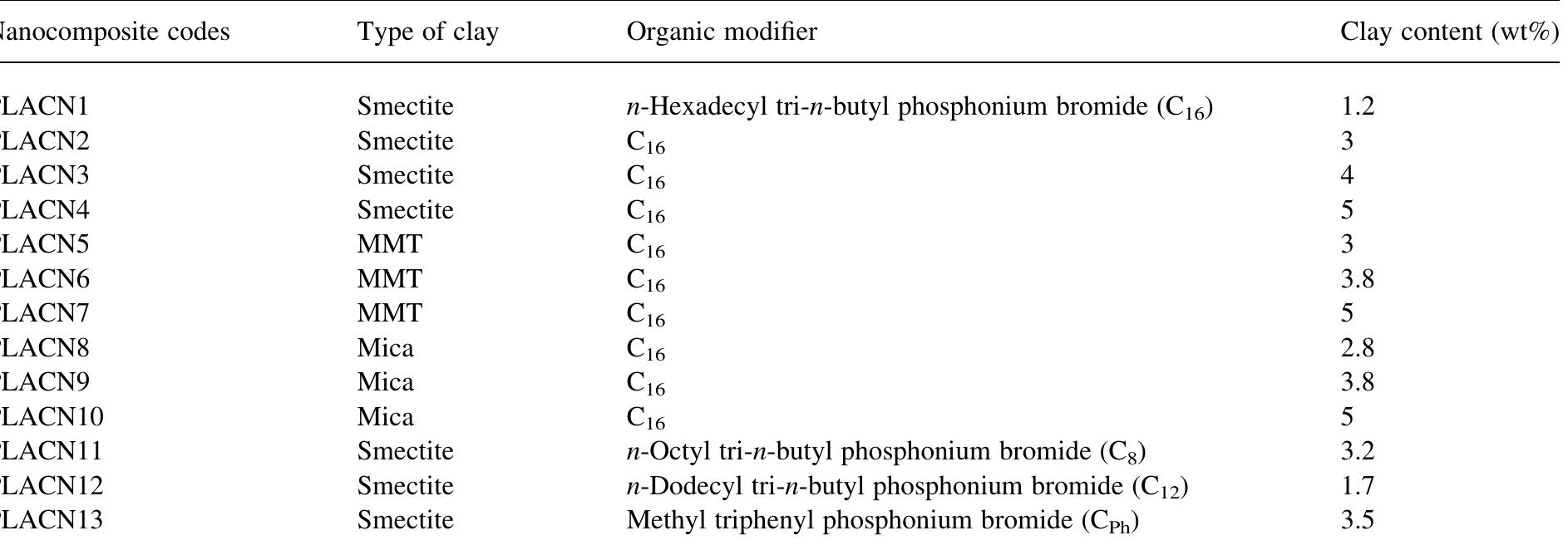


![G' value of various PLACNs and corresponding matrices without clay at different temperature range [374] Reproduced from Sinha Ray, Maiti, Okamoto, Yamada and Ueda by permission of American Chemical Society, USA.](https://figures.academia-assets.com/30475323/table_014.jpg)

![Reproduced from Fornes, Yoon, Keskkula and Paul by permission of Elsevier Science Ltd, UK. * Strain at yield point measured during modulus and yield strength testing using a crosshead speed of 0.51 cm/min. Mechanical properties of some N6/(HE)2M,R; nanocomposites [149]](https://figures.academia-assets.com/30475323/table_016.jpg)
![Reproduced from Lee, Park, Lim, Kang, Li, Cho and Ha by permission of Elsevier Science Ltd, UK. Tensile properties of APES/Closite 30B nanocomposites [398]](https://figures.academia-assets.com/30475323/table_017.jpg)
![Reproduced from Sinha Ray, Yamada, Okamoto and Ueda by permission of Elsevier Science Ltd, UK. Comparison of materials properties between neat PLA and various PLACNs prepared with octadecyltrimethylammonium modified MMT [386]](https://figures.academia-assets.com/30475323/table_018.jpg)
![HDT of PP/MMT nanocomposites and the respective unfilled PP [305] Table 18](https://figures.academia-assets.com/30475323/table_019.jpg)
![Heat flux, 35 kW/m’. H,, specific heat of combustion; SEA, specific extinction area. Peak HRR, mass loss rate, and SEA data, measured at 35 kW/m”, are reproducible to within + 10%. The carbon monoxide and heat of combustion data are reproducible to within +15%. Reproduced from Gilman, Jackson, Morgan, Harris Jr, Manias, Giannelis, Wuthemow, Hilton and Phillips by permission of American Chemical Society, USA. Cone calorimeter data of various polymers and their nanocomposites with OMLS [17]](https://figures.academia-assets.com/30475323/table_020.jpg)
![Reproduced from Nam, Maiti, Okamoto, Kotaka, Nakayama, Takada, Ohshima, Usuki, Hasegawa and Okamoto by permission of Society of Plastics Engineers. Characteristic parameters of pre- and post-foamed PP-MA and various PPCNs [313]](https://figures.academia-assets.com/30475323/table_021.jpg)